


Epson Research and Development
Page 13
Vancouver Design Center
S5U13505B00C Rev. 1.0 ISA Bus Evaluation Board User Manual S1D13505
Issue Date: 01/02/05 X23A-G-004-05
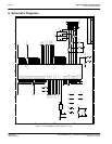
6 Technical Description
6.1 ISA Bus Support
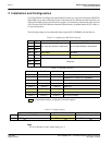
The S5U13505B00C directly supports the 16-bit ISA bus environment. All the configuration options
[MD15:0] are either hard-wired or selectable through the eight-position DIP Switch S1. Refer to
Table 2-1 “Configuration DIP Switch Settings” on page 8 for details.
Note
1. This evaluation board supports a 16-bit ISA bus only.
2. The S1D13505 is a memory-mapped device with 2M bytes of linear addressed display buffer
and a separate 47 byte register space. On the S5U13505B00C, the S1D13505 2M byte display
buffer has been mapped to a start address of C00000h and the registers have been mapped to a
start address of E00000h.
3. When using this board in a PC environment, system memory must be limited to 12M bytes, to
prevent the system addresses will conflict with the S1D13505 display buffer/register
addresses.
4. The hardware suspend enable/disable address is at location F00000h. A read to this location
will enable the hardware suspend, a write to the same location will disable it.
Note
Due to backwards compatibility with the S5U13505B00B Evaluation Board, which supports
both an 8 and a 16-bit CPU interface, third party software
must
perform a write at address
F80000h in order to enable a 16-bit ISA environment. This must be done prior to initializing the
S1D13505. Failure to do so will result in the S1D13505 being configured as a 16-bit device (de-
fault, power-up), with the ISA Bus interface (supported through the PAL (U4)) configured for an
8-bit
interface.
The Epson supplied software performs this function automatically.
6.2 Non-ISA Bus Support
This evaluation board is specifically designed to support the standard 16-bit ISA bus. However, the
S1D13505 directly supports many other host bus interfaces. Header strips H1 and H2 have been
provided and contain all the necessary I/O pins to interface to these buses. See, Section 4 “CPU/Bus
Interface Connector Pinouts” on page 10, Table 2-1 “Configuration DIP Switch Settings” on page
8, and Table 2-3 “Jumper Settings” on page 8, for details.