


Page 16
Epson Research and Development
Vancouver Design Center
S1D13505 Interfacing to the PC Card Bus
X23A-G-005-06 Issue Date: 01/02/05
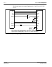
4.4 Register/Memory Mapping
The S1D13505 is a memory mapped device. The internal registers require 47 bytes and are
mapped in the lower PC Card memory address space starting at zero.The display buffer
requires 2M bytes and is mapped in the third and fourth megabytes of the PC Card address
space (ranging from 200000h to 3FFFFFh).
A typical implementation as shown in Figure 4-1: “Typical Implementation of PC Card to
S1D13505 Interface,” on page 14 has Chip Select (CS#) connected to ground (always
enabled) and the Memory/Register select pin (M/R#) connected to address bit A21. This
provides the following decoding:
The PC Card socket provides 64M byte of address space. Without further resolution on the
decoding logic (M/R# connected to A21), the entire register set is aliased for every 64 byte
boundary within the specified address range above. Since address bits A[25:22] are
ignored, the S1D13505 registers and display buffer are aliased 16 times.
Note
If aliasing is not desirable, the upper addresses must be fully decoded.
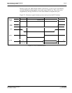
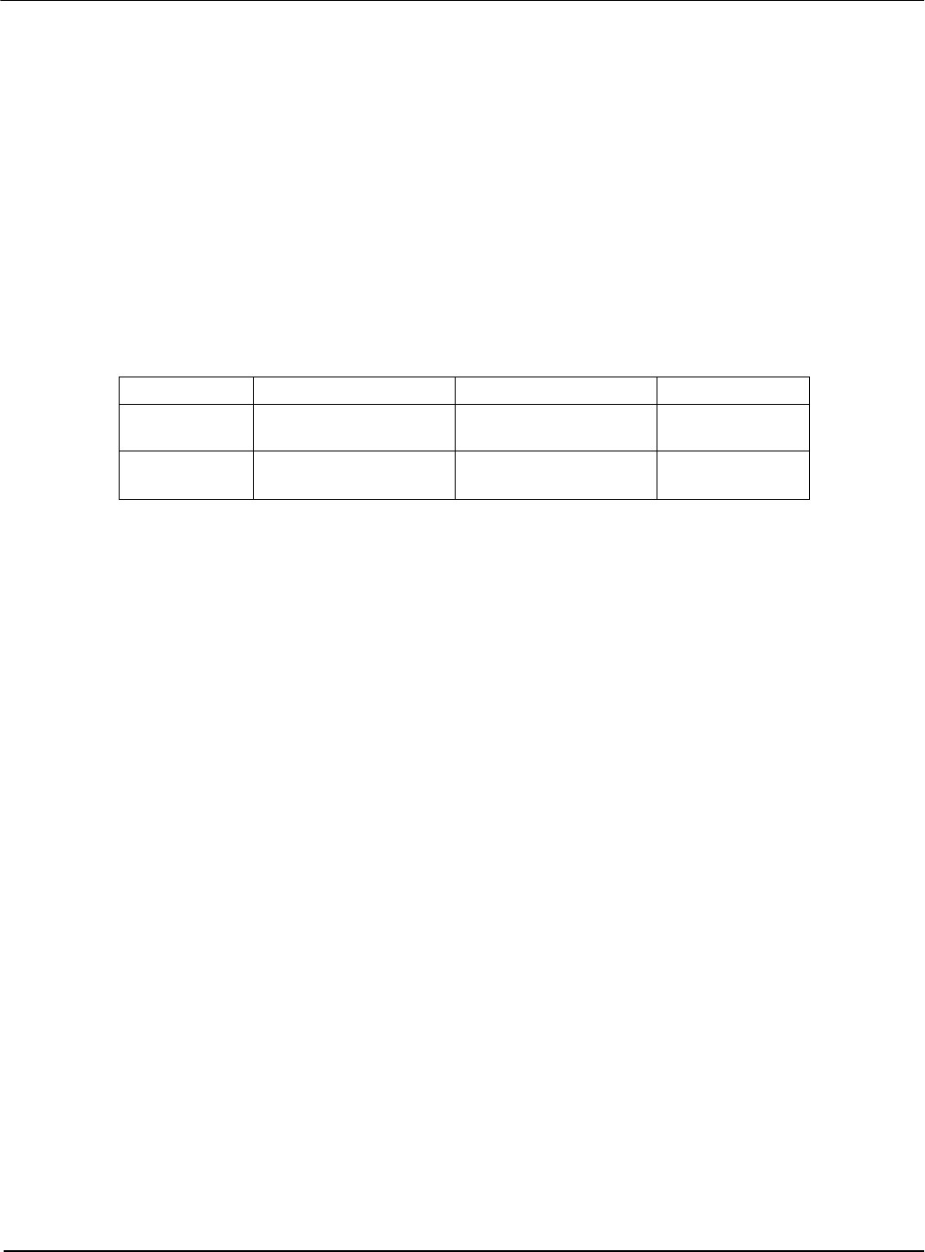
Table 4-2: Register/Memory Mapping for Typical Implementation
CS# M/R# (A21) Address Range Function
0 0 0 - 1F FFFFh
Internal Register
Set decoded
0 1 20 0000h - 3F FFFFh
Display Buffer
decode