


Page 20
Epson Research and Development
Vancouver Design Center
S1D13505 Interfacing to the Motorola MPC821 Microprocessor
X23A-G-008-05 Issue Date: 01/02/05
4.6 Test Software
The test software is very simple. It configures chip select 4 (CS4) on the MPC821 to map
the S1D13505 to an unused 4M byte block of address space. Next, it loads the appropriate
values into the option register for CS4 and writes the value 0 to the S1D13505 register
REG[1Bh] to enable the S1D13505 host interface. Lastly, the software runs a tight loop that
reads the S1D13505 Revision Code Register REG[00h]. This allows monitoring of the bus
timing on a logic analyzer.
The following source code was entered into the memory of the MPC821ADS using the
line-by-line assembler in MPC8BUG (the debugger provided with the ADS board). Once
the program was executed on the ADS, a logic analyzer was used to verify operation of the
interface hardware.
It is important to note that when the MPC821 comes out of reset, the on-chip caches and
MMU are disabled. If the data cache is enabled, then the MMU must be set so that the
S1D13505 memory block is tagged as non-cacheable. This ensures the MPC821 does not
attempt to cache any data read from, or written to, the S1D13505 or its display buffer.
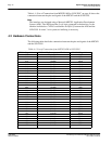
BR4 equ $120 ; CS4 base register
OR4 equ $124 ; CS4 option register
MemStart equ $40 ; upper word of S1D13505 start address
DisableReg equ $1b ; address of S1D13505 Disable Register
RevCodeReg equ 0 ; address of Revision Code Register
Start mfspr r1,IMMR ; get base address of internal registers
andis. r1,r1,$ffff ; clear lower 16 bits to 0
andis. r2,r0,0 ; clear r2
oris r2,r2,MemStart ; write base address
ori r2,r2,$0801 ; port size 16 bits; select GPCM; enable
stw r2,BR4(r1) ; write value to base register
andis. r2,r0,0 ; clear r2
oris r2,r2,$ffc0 ; address mask – use upper 10 bits
ori r2,r2,$0608 ; normal CS negation; delay CS ½ clock;
; no burst inhibit (13505 does this)
stw r2,OR4(r1) ; write to option register
andis. r1,r0,0 ; clear r1
oris r1,r1,MemStart ; point r1 to start of S1D13505 mem space
stb r1,DisableReg(r1) ; write 0 to disable register
Loop lbz r0,RevCodeReg(r1) ; read revision code into r1
b Loop ; branch forever
end
Note
MPC8BUG does not support comments or symbolic equates; these have been added for
clarity.