


Page 30
Epson Research and Development
Vancouver Design Center
S1D13505 Hardware Functional Specification
X23A-A-001-14 Issue Date: 01/02/02
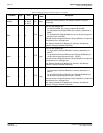
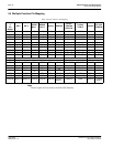
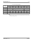
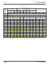
MA[8:0] O
58, 60, 62,
64, 66, 67,
65, 63, 61
CO1 0utput
Multiplexed memory address - see
Memory Interface Timing
for
functionality.
MA9 IO 56
C/TS
1
0utput
This is a multi-purpose pin:
• For 2M byte DRAM, this is memory address bit 9 (MA9).
• For asymmetrical 512K byte DRAM, this is memory address bit 9
(MA9).
• For symmetrical 512K byte DRAM, this pin can be used as general
purpose IO pin 3 (GPIO3).
Note that unless configured otherwise, this pin defaults to an input and
must be driven to a valid logic level.
See
“Memory Interface Pin Mapping”
for summary. See
Memory
Interface Timing
for detailed functionality.
MA10 IO 59
C/TS
1
0utput
This is a multi-purpose pin:
• For asymmetrical 2M byte DRAM this is memory address bit 10
(MA10).
• For symmetrical 2M byte DRAM and all 512K byte DRAM this pin
can be used as general purpose IO pin 1 (GPIO1).
Note that unless configured otherwise, this pin defaults to an input and
must be driven to a valid logic level.
See
“Memory Interface Pin Mapping”
for summary. See
Memory
Interface Timing
for detailed functionality.
MA11 IO 57
C/TS
1
0utput
This is a multi-purpose pin:
• For asymmetrical 2M byte DRAM this is memory address bit 11
(MA11).
• For symmetrical 2M byte DRAM and all 512K byte DRAM this pin
can be used as general purpose IO pin 2 (GPIO2).
Note that unless configured otherwise, this pin defaults to an input and
must be driven to a valid logic level.
See
“Memory Interface Pin Mapping”
for summary. See
Memory
Interface Timing
for detailed functionality.
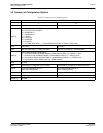
Table 5-2: Memory Interface Pin Descriptions (Continued)
Pin Name Type Pin # Cell
RESET#
State
Description