


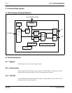

Page 28
Epson Research and Development
Vancouver Design Center
S1D13505 Hardware Functional Specification
X23A-A-001-14 Issue Date: 01/02/02
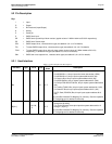
WAIT# O 15
TS2 Hi-Z
The active polarity of the WAIT# output is configurable; the state of MD5
on the rising edge of RESET# defines the active polarity of WAIT# - see
“Summary of Configuration Options”
.
• For SH-3 Bus, this pin outputs the wait request signal (WAIT#); MD5
must be pulled low during reset by the internal pull-down resistor.
• For SH-4 Bus, this pin outputs the ready signal (RDY#); MD5 must be
pulled high during reset by an external pull-up resistor.
• For MC68K Bus 1, this pin outputs the data transfer acknowledge
signal (DTACK#); MD5 must be pulled high during reset by an
external pull-up resistor.
• For MC68K Bus 2, this pin outputs the data transfer and size
acknowledge bit 1 (DSACK1#); MD5 must be pulled high during reset
by an external pull-up resistor.
• For Generic Bus, this pin outputs the wait signal (WAIT#); MD5 must
be pulled low during reset by the internal pull-down resistor.
• For MIPS/ISA Bus, this pin outputs the IO channel ready signal
(IOCHRDY); MD5 must be pulled low during reset by the internal pull-
down resistor.
• For Philips PR31500/31700 Bus, this pin outputs the wait state signal
(/CARDxWAIT); MD5 must be pulled low during reset by the internal
pull-down resistor.
• For Toshiba TX3912 Bus, this pin outputs the wait state signal
(CARDxWAIT*); MD5 must be pulled low during reset by the internal
pull-down resistor.
• For PowerPC Bus, this pin outputs the transfer acknowledge signal
(TA#); MD5 must be pulled high during reset by an external pull-up
resistor.
• For PC Card (PCMCIA) Bus, this pin outputs the wait signal (-WAIT);
MD5 must be pulled low during reset by the internal pull-down
resistor.
See
“Host Bus Interface Pin Mapping”
for summary. See the respective
AC Timing diagram for detailed functionality.
RESET# I 11
CS 0
Active low input that clears all internal registers and forces all outputs to
their inactive states. Note that active high RESET signals must be
inverted before input to this pin.
Table 5-1: Host Interface Pin Descriptions (Continued)
Pin Name Type Pin # Cell
RESET#
State
Description