


Page 8
Epson Research and Development
Vancouver Design Center
S1D13505 Interfacing to the PC Card Bus
X23A-G-005-06 Issue Date: 01/02/05
2 Interfacing to the PC Card Bus
2.1 The PC Card System Bus
PC Card technology has gained wide acceptance in the mobile computing field as well as
in other markets due to its portability and ruggedness. This section is an overview of the
operation of the 16-bit PC Card interface conforming to the PCMCIA 2.0/JEIDA 4.1
Standard (or later).
2.1.1 PC Card Overview
The 16-bit PC Card provides a 26-bit address bus and additional control lines which allow
access to three 64M byte address ranges. These ranges are used for common memory space,
IO space, and attribute memory space. Common memory may be accessed by a host system
for memory read and write operations. Attribute memory is used for defining card specific
information such as configuration registers, card capabilities, and card use. IO space
maintains software and hardware compatibility with hosts such as the Intel x86
architecture, which address peripherals independently from memory space.
Bit notation follows the convention used by most micro-processors, the high bit being the
most significant. Therefore, signals A25 and D15 are the most significant bits for the
address and data busses respectively.
Support is provided for on-chip DMA controllers. To find further information on these
topics, refer to Section 6, “References” on page 18.
PC Card bus signals are asynchronous to the host CPU bus signals. Bus cycles are started
with the assertion of the CE1# and/or the CE2# card enable signals. The cycle ends once
these signals are de-asserted. Bus cycles can be lengthened using the WAIT# signal.
Note
The PCMCIA 2.0/JEIDA 4.1 (and later) PC Card Standard support the two signals
WAIT# and RESET which are not supported in earlier versions of the standard. The
WAIT# signal allows for asynchronous data transfers for memory, attribute, and IO
access cycles. The RESET signal allows resetting of the card configuration by the reset
line of the host CPU.
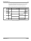
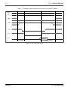
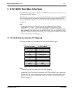
2.1.2 Memory Access Cycles
A data transfer is initiated when a memory address is placed on the PC Card bus and one,
or both, of the card enable signals (CE1# and CE2#) are driven low. REG# must be inactive.
If only CE1# is driven low, 8-bit data transfers are enabled and A0 specifies whether the
even or odd data byte appears on data bus lines D[7:0]. If both CE1# and CE2# are driven
low, a 16-bit word transfer takes place. If only CE2# is driven low, an odd byte transfer
occurs on data lines D[15:8].