


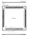

Page 26
Epson Research and Development
Vancouver Design Center
S1D13505 Hardware Functional Specification
X23A-A-001-14 Issue Date: 01/02/02
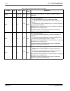
BUSCLK I 13
CHi-Z
This pin inputs the system bus clock. It is possible to apply a 2x clock
and divide it by 2 internally - see MD12 in
Summary of Configuration
Options
.
• For SH-3/SH-4 Bus, this pin is connected to CKIO.
• For MC68K Bus 1, this pin is connected to CLK.
• For MC68K Bus 2, this pin is connected to CLK.
• For Generic Bus, this pin is connected to BCLK.
• For MIPS/ISA Bus, this pin is connected to CLK.
• For Philips PR31500/31700 Bus, this pin is connected to DCLKOUT.
• For Toshiba TX3912 Bus, this pin is connected to DCLKOUT.
• For PowerPC Bus, this pin is connected to CLKOUT.
• For PC Card (PCMCIA) Bus, this pin is connected to CLKI.
See
“Host Bus Interface Pin Mapping”
for summary. See the respective
AC Timing diagram for detailed functionality.
BS# I 6
CS Hi-Z
This is a multi-purpose pin:
• For SH-3/SH-4 Bus, this pin inputs the bus start signal (BS#).
• For MC68K Bus 1, this pin inputs the address strobe (AS#).
• For MC68K Bus 2, this pin inputs the address strobe (AS#).
• For Generic Bus, this pin is connected to V
DD
.
• For MIPS/ISA Bus, this pin is connected to V
DD
.
• For Philips PR31500/31700 Bus, this pin is connected to V
DD
.
• For Toshiba TX3912 Bus, this pin is connected to V
DD
.
• For PowerPC Bus, this pin inputs the Transfer Start signal (TS#).
• For PC Card (PCMCIA) Bus, this pin is connected to V
DD
.
See
“Host Bus Interface Pin Mapping”
for summary. See the respective
AC Timing diagram for detailed functionality.
RD/WR# I 10
CS Hi-Z
This is a multi-purpose pin:
• For SH-3/SH-4 Bus, this pin inputs the read write signal (RD/WR#).
The S1D13505 needs this signal for early decode of the bus cycle.
• For MC68K Bus 1, this pin inputs the read write signal (R/W#).
• For MC68K Bus 2, this pin inputs the read write signal (R/W#).
• For Generic Bus, this pin inputs the read command for the upper data
byte (RD1#).
• For MIPS/ISA Bus, this pin is connected to V
DD
.
• For Philips PR31500/31700 Bus, this pin inputs the even byte access
enable signal (/CARDxCSL).
• For Toshiba TX3912 Bus, this pin inputs the even byte access enable
signal (CARDxCSL*).
• For PowerPC Bus, this pin inputs the read write signal (RD/WR#).
• For PC Card (PCMCIA) Bus, this pin inputs the card enable 1 signal
(-CE1).
See
“Host Bus Interface Pin Mapping”
for summary. See the respective
AC Timing diagram for detailed functionality.
Table 5-1: Host Interface Pin Descriptions (Continued)
Pin Name Type Pin # Cell
RESET#
State
Description