


Epson Research and Development
Page 33
Vancouver Design Center
Hardware Functional Specification S1D13505
Issue Date: 01/02/02 X23A-A-001-14
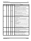
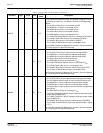
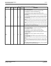
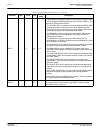
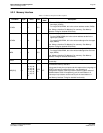
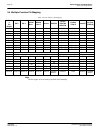
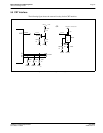
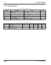
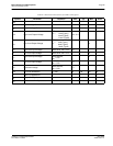
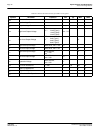
5.3 Summary of Configuration Options
Table 5-5: Summary of Power On/Reset Options
Pin Name value on this pin at rising edge of RESET# is used to configure:
(1/0)
10
MD0 8-bit host bus interface 16-bit host bus interface
MD[3:1]
Select host bus interface:MD[11] = 0:
000 = SH-3/SH-4 bus interface
001 = MC68K Bus 1
010 = MC68K Bus 2
011 = Generic
100 = Reserved
101 = MIPS/ISA
110 = PowerPC
111 = PC Card (when MD11 = 1 Philips PR31500/PR31700 or Toshiba TX3912 Bus)
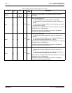
MD4 Little Endian Big Endian
MD5 WAIT# is active high (1 = insert wait state) WAIT# is active low (0 = insert wait state)
MD[7:6]
Memory Address/GPIO configuration:
00 = symmetrical 256K
×
16 DRAM. MA[8:0] = DRAM address. MA[11:9] = GPIO2,1,3 pins.
01 = symmetrical 1M
×
16 DRAM. MA[9:0] = DRAM address. MA[10:11] = GPIO2,1 pins.
10 = asymmetrical 256K
×
16 DRAM. MA[9:0] = DRAM address. MA[10:11] = GPIO2,1 pins.
11 = asymmetrical 1M
×
16 DRAM. MA[11:0] = DRAM address.
MD8 Not used
MD9 SUSPEND# pin configured as GPO output SUSPEND# pin configured as SUSPEND# input
MD10
Active low LCDPWR polarity or
active high GPO polarity
Active high LCDPWR polarity or
active low GPO polarity
MD11 Alternate Host Bus Interface Selected Primary Host Bus Interface Selected
MD12 BUSCLK input divided by 2 BUSCLK input not divided
MD[15:13] Not used