


Epson Research and Development
Page 13
Vancouver Design Center
Interfacing to the NEC VR4121™ Microprocessor S1D13505
Issue Date: 01/02/05 X23A-G-011-04
4.2 S1D13505 Configuration
The S1D13505 latches MD15 through MD0 to allow selection of the bus mode and other
configuration data on the rising edge of RESET#. For details on configuration, refer to the
S1D13505 Hardware Functional Specification, document number X23A-A-001-xx.
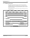
The table below shows those configuration settings relevant to the MIPS/ISA host bus
interface used by the NEC V
R
4121 microprocessor.
4.3 NEC V
R
4121
Configuration
The NEC V
R
4121 register BCUCNTREG1 bit ISAM/LCD must be set to 0. A 0 indicates
that the reserved address space is for the LCD controller, and not for the high-speed ISA
memory. The register BCUCNTREG2 bit GMODE must be set to 1 to indicate that a
non-inverting data bus is used for LCD controller accesses.
The LCD interface must be set to operate using a 16-bit data bus. This is accomplished by
setting the NEC V
R
4121 register BCUCNTREG3 bit LCD32/ISA32 to 0.
Note
Setting the register BCUCNTREG3 bit LCD32/ISA32 to 0 affects both the LCD con-
troller and high-speed ISA memory access.
The frequency of BUSCLK output is programmed from the state of pins TxD/CLKSEL2,
RTS#/CLKSEL1 and DTR#/CLKSEL0 during reset, and from the PMU (Power
Management Unit) configuration registers of the NEC V
R
4121. The S1D13505 works at
any of the frequencies provided by the NEC V
R
4121.
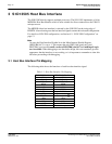
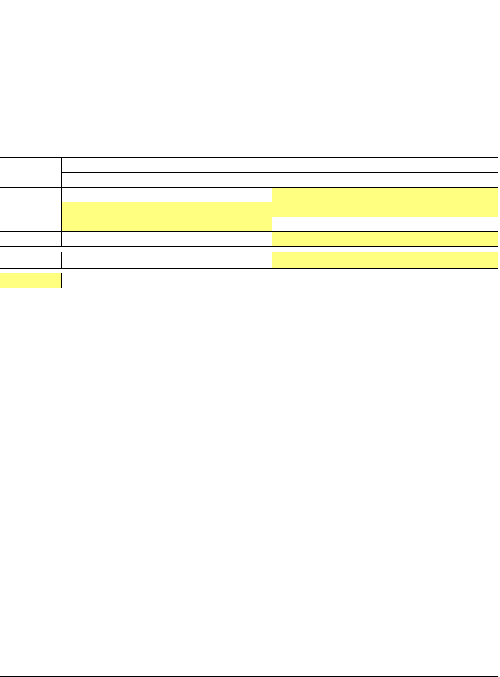
Table 4-1: Summary of Power-On-Reset Options
S1D13505
Pin Name
value on this pin at rising edge of RESET# is used to configure:
(1/0)
10
MD0 8-bit host bus interface 16-bit host bus interface
MD[3:1]
101 = MIPS/ISA host bus interface
MD4
Little Endian Big Endian
MD5 WAIT# is active high (1 = insert wait state)
WAIT# is active low (0 = insert wait state)
MD11 Alternate Host Bus Interface Selected Primary Host Bus Interface Selected
= configuration for NEC VR4121 microprocessor