


Page 110
Epson Research and Development
Vancouver Design Center
S1D13505 Hardware Functional Specification
X23A-A-001-14 Issue Date: 01/02/02
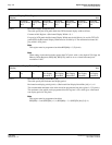
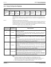
8.2.5 Clock Configuration Register
bit 7 Reserved
This bit must be set to 0.
Note
There must always be a source clock at CLKI.
bit 2 MCLK Divide Select
When this bit = 1 the MCLK frequency is half of its source frequency.
When this bit = 0 the MCLK frequency is equal to its source frequency.
The MCLK frequency should always be set to the maximum frequency allowed by the DRAM; this
provides maximum performance and minimum overall system power consumption.
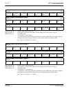
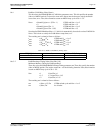
bits 1-0 PCLK Divide Select Bits [1:0]
These bits select the MCLK: PCLK frequency ratio
See section on “
Maximum MCLK:PCLK Frequency Ratios
” for selection of clock ratios.
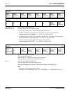
8.2.6 Power Save Configuration Registers
bit 7 Power Save Status
This is a read-only status bit.
This bit indicates the power-save state of the chip.
When this bit = 1, the panel has been powered down and the memory controller is either in self
refresh mode or is performing only
CAS-before-RAS
refresh cycles.
When this bit = 0, the chip is either powered up, in transition of powering up, or in transition of
powering down. See Section 15
Power Save Modes
for details.
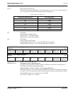
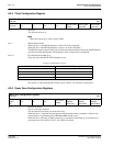
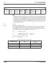
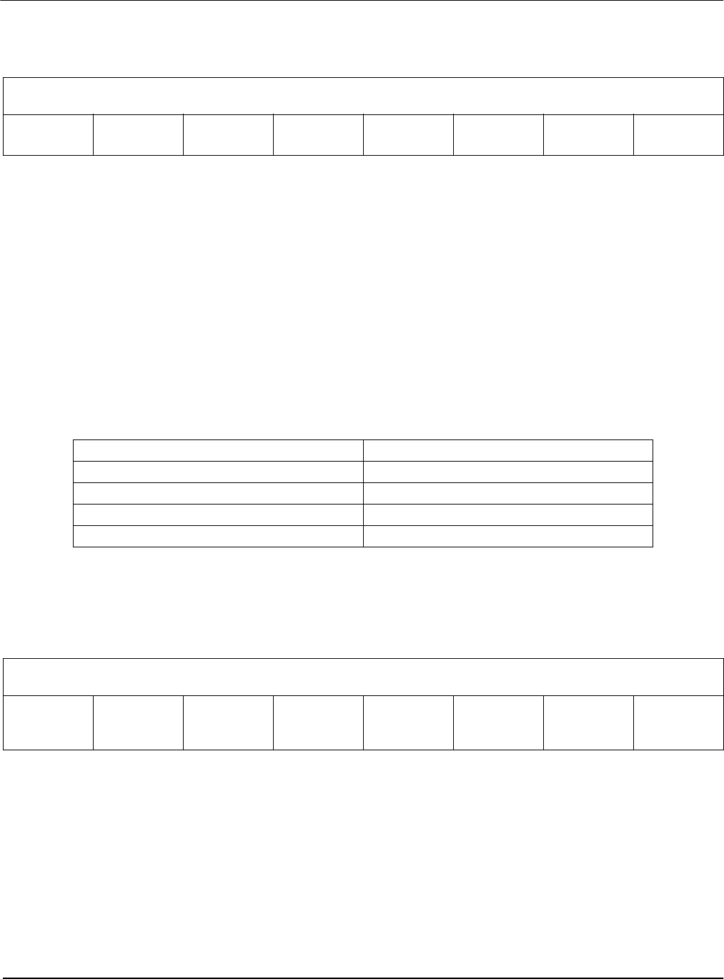
Clock Configuration Register
REG[19h] RW
Reserved n/a n/a n/a n/a
MCLK Divide
Select
PCLK Divide
Select Bit 1
PCLK Divide
Select Bit 0
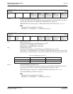
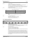
Table 8-9: PCLK Divide Selection
PCLK Divide Select Bits [1:0] MCLK: PCLK Frequency Ratio
00 1: 1
01 2: 1
10 3: 1
11 4: 1
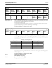
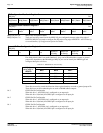
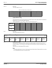
Power Save Configuration Register
REG[1Ah] RW
Power Save
Status
RO
n/a n/a n/a
LCD Power
Disable
Suspend
Refresh
Select Bit 1
Suspend
Refresh
Select Bit 0
Software
Suspend
Mode Enable