


Epson Research and Development
Page 31
Vancouver Design Center
Hardware Functional Specification S1D13505
Issue Date: 01/02/02 X23A-A-001-14
5.2.3 LCD Interface
5.2.4 CRT Interface
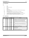
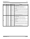
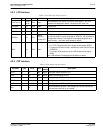
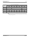
Table 5-2: LCD
Interface Pin Descriptions
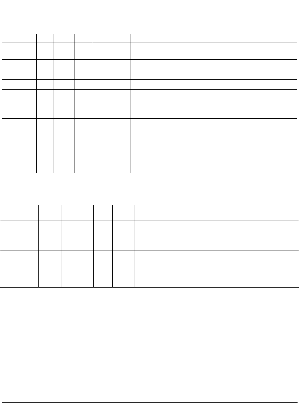
Pin Name Type Pin # Cell RESET# State Description
FPDAT[15:0] O
95-88,
86-79
CN3 0utput
Panel data bus. Not all pins are used for some panels - see
LCD
Interface Pin Mapping
for details. Unused pins are driven low.
FPFRAME O 73 CN3 0utput Frame pulse
FPLINE O 74 CN3 0utput Line pulse
FPSHIFT O 77 CO3 0utput Shift clock
LCDPWR O 75 CO1
0utput if
MD[10]=0
1 if MD[10]=1
LCD power control output. The active polarity of this output is selected
by the state of MD10 at the rising edge of RESET# - see
Summary of
Configuration Options
. This output is controlled by the power save
mode circuitry - see
Power Save Modes
for details.
DRDY O 76 CN3 0utput
This is a multi-purpose pin:
• For TFT/D-TFD panels this is the display enable output (DRDY).
• For passive LCD with Format 1 interface this is the 2nd Shift Clock
(FPSHIFT2)
• For all other LCD panels this is the LCD backplane bias signal
(MOD).
See
LCD Interface Pin Mapping
and REG[02h] for details.
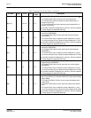
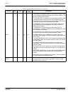
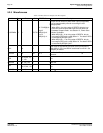
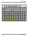
Table 5-3: CRT Interface Pin Descriptions
Pin Name Type Pin # Cell
RESET
# State
Description
HRTC IO 107 CN3 0utput Horizontal retrace signal for CRT
VRTC IO 108 CN3 0utput Vertical retrace signal for CRT
RED O 100 A Analog output for CRT color Red
GREEN O 103 A Analog output for CRT color Green
BLUE O 105 A Analog output for CRT color Blue
IREF I 101 A
Current reference for DAC - see
Analog Pins
. This pin must be left
unconnected if the DAC is not needed.