


Page 70
Epson Research and Development
Vancouver Design Center
S1D13505 Hardware Functional Specification
X23A-A-001-14 Issue Date: 01/02/02
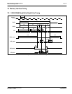
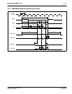
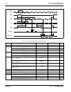
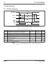
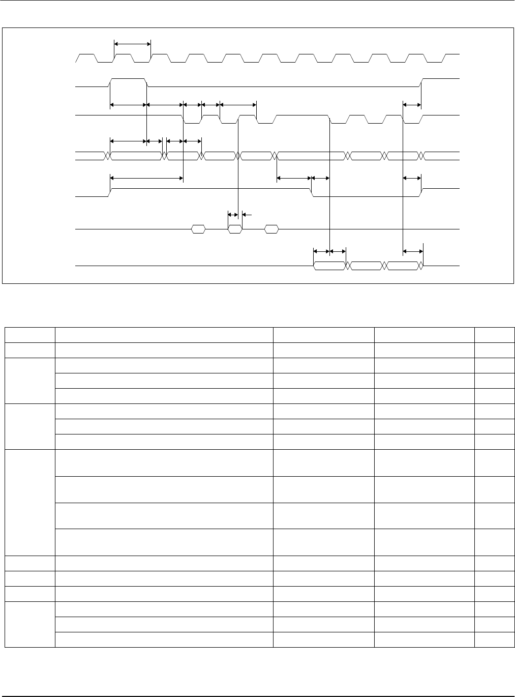
Figure 7-19: FPM-DRAM Read-Write Timing
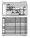
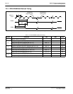
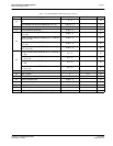
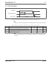
Table 7-18: FPM-DRAM Read/Write/Read-Write Timing
Symbol Parameter Min Max Units
t1 Internal memory clock period 40 ns
t2
Random read cycle REG[22h] bit 6-5 == 00 5t1 ns
Random read cycle REG[22h] bit 6-5 == 01 4t1 ns
Random read cycle REG[22h] bit 6-5 == 10 3t1 ns
t3
RAS# precharge time (REG[22h] bits 3-2 = 00) 2 t1 - 3 ns
RAS# precharge time (REG[22h] bits 3-2 = 01) 1.45 t1 - 3 ns
RAS# precharge time (REG[22h] bits 3-2 = 10) 1 t1 - 3 ns
t4
RAS# to CAS# delay time (REG[22h] bit 4 = 1 and
bits 3-2 = 00 or 10)
1.45 t1 - 3 ns
RAS# to CAS# delay time (REG[22h] bit 4 = 0 and
bits 3-2 = 00 or 10)
2.45 t1 - 3 ns
RAS# to CAS# delay time (REG[22h] bit 4 = 1 and
bits 3-2 = 01)
1t1 - 3 ns
RAS# to CAS# delay time (REG[22h] bit 4 = 0 and
bits 3-2 = 01)
2t1 - 3 ns
t5 CAS# precharge time 0.45 t1 - 3 ns
t6 CAS# pulse width 0.45 t1 - 3 ns
t7 RAS# hold time 0.45 t1 - 3 ns
t8
Row address setup time (REG[22h] bits 3-2 = 00) 2 t1 - 3 ns
Row address setup time (REG[22h] bits 3-2 = 01) 1.45 t1 - 3 ns
Row address setup time (REG[22h] bits 3-2 = 10) 1 t1 - 3 ns
RAS#
CAS#
MA
MD(read)
R
C1
Memory
Clock
d1
C2 C3
d2 d3
t3
t4
t5
t6
t1
t7
t8
t9
t10 t11
t14 t15
t21 t16
WE#
t12 t17
t1
MD(write)
t18 t19
d1 d2 d3
t20
C2 C3C1