


Page 112
Epson Research and Development
Vancouver Design Center
S1D13505 Hardware Functional Specification
X23A-A-001-14 Issue Date: 01/02/02
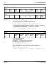
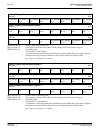
REG[1Ch] bits 7-0 MD[15:0] Configuration Status
REG[1Dh] bits 7-0 These are read-only status bits for the MD[15:0] pins configuration status at the rising edge of
RESET#. MD[15:0] are used to configure the chip at the rising edge of RESET# – see
Pin Descrip-
tions
and
Summary of Configuration Options
for details.
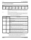
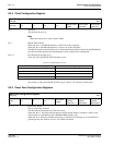
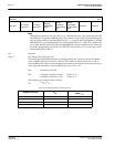
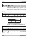
Pins MA9, MA10, MA11 are multi-functional – they can be DRAM address outputs or general
purpose IO dependent on the DRAM type. MD[7:6] are used to identify the DRAM type and
configure these pins as follows:
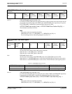
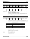
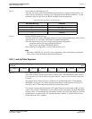
These bits are used to control the direction of these pins when they are used as general purpose IO.
These bits have no effect when the pins are used as DRAM address outputs.
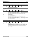
bit 3 GPIO3 Pin IO Configuration
When this bit = 1, the GPIO3 pin is configured as an output pin.
When this bit = 0 (default), the GPIO3 pin is configured as an input pin.
bit 2 GPIO2 Pin IO Configuration
When this bit = 1, the GPIO2 pin is configured as an output pin.
When this bit = 0 (default), the GPIO2 pin is configured as an input pin.
bit 1 GPIO1 Pin IO Configuration
When this bit = 1, the GPIO1 pin is configured as an output pin.
When this bit = 0 (default), the GPIO1 pin is configured as an input pin.
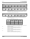
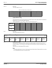
MD Configuration Readback Register 0
REG[1Ch] RO
MD[7] Status MD[6] Status MD[5] Status MD[4] Status MD[3] Status MD[2] Status MD[1] Status MD[0] Status
MD Configuration Readback Register 1
REG[1Dh] RO
MD[15]
Status
MD[14]
Status
MD[13]
Status
MD[12]
Status
MD[11]
Status
MD[10]
Status
MD[9]
Status
MD[8]
Status
General IO Pins Configuration Register 0
REG[1Eh] RW
n/a n/a n/a n/a
GPIO3 Pin
IO Config.
GPIO2 Pin
IO Config.
GPIO1 Pin
IO Config.
n/a
Table 8-11: MA/GPIO Pin Functionality
MD[7:6] at
rising edge of
RESET#
Pin Function
MA9 MA10 MA11
00 GPIO3 GPIO1 GPIO2
01 MA9 GPIO1 GPIO2
10 MA9 GPIO1 GPIO2
11 MA9 MA10 MA11