


Epson Research and Development
Page 115
Vancouver Design Center
Hardware Functional Specification S1D13505
Issue Date: 01/02/02 X23A-A-001-14
bit 4 RAS#-to-CAS# Delay Value (N
RCD
)
This bit selects the DRAM RAS#-to-CAS# delay parameter, t
RCD
. This bit specifies the number
(N
RCD
) of MCLK periods (T
M
) used to create t
RCD
. N
RCD
must be chosen to satisfy the RAS#
access time, t
RAC
. Note, these formulae assume an MCLK duty cycle of 50 +/- 5%.
N
RCD
= Round-Up((t
RAC
+ 5)/T
M
- 1) if EDO and N
RP
= 1 or 2
= 2 if EDO and N
RP
= 1.5
= Round-Up(t
RAC
/T
M
- 1) if FPM and N
RP
= 1 or 2
= Round-Up(t
RAC
/T
M
- 0.45) if FPM and N
RP
= 1.5
Note that for EDO-DRAM and N
RP
= 1.5, this bit is automatically forced to 0 to select 2 MCLK for
N
RCD
. This is done to satisfy the CAS# address setup time, t
ASC
.
The resulting t
RC
is related to N
RCD
as follows:
t
RCD
= (N
RCD
) T
M
if EDO and N
RP
= 1 or 2
t
RCD
= (1.5) T
M
if EDO and N
RP
= 1.5
t
RCD
= (N
RCD
+ 0.5) T
M
if FPM and N
RP
= 1 or 2
t
RCD
= (N
RCD
) T
M
if FPM and N
RP
= 1.5
bits 3-2 RAS# Precharge Timing Value (N
RP
) Bits [1:0]
Minimum Memory Timing for RAS# precharge
These bits select the DRAM RAS# Precharge timing parameter, t
RP
. These bits specify the number
(N
RP
) of MCLK periods (T
M
) used to create t
RP
– see the following formulae. Note, these formulae
assume an MCLK duty cycle of 50 +/- 5%.
N
RP
= 1 if (t
RP
/T
M
) < 1
= 1.5 if 1
≤
(t
RP
/T
M
) < 1.45
= 2 if (t
RP
/T
M
)
≥
1.45
The resulting t
RC
is related to N
RP
as follows:
t
RP
= (N
RP
+ 0.5) T
M
if FPM refresh cycle and N
RP
= 1 or 2
t
RP
= (N
RP
) T
M
for all other
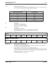
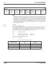
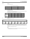
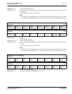
Table 8-13: RAS#-to-CAS# Delay Timing Select
REG[22h] bit 4 N
RCD
RAS#-to-CAS# Delay (t
RCD
)
022
111