


Epson Research and Development
Page 71
Vancouver Design Center
Hardware Functional Specification S1D13505
Issue Date: 01/02/02 X23A-A-001-14
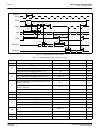
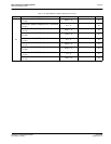
t9
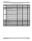
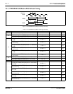
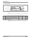
Row address hold time (REG[22h] bits 3-2 = 00 or
10)
t1 - 3 ns
Row address hold time (REG[22h] bits 3-2 = 01) 0.45 1t1 - 3 ns
t10 Column address setup time 0.45 t1 - 3 ns
t11 Column address hold time 0.45 t1 - 3 ns
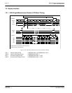
t12
Read Command Setup (REG[22h] bit 4 = 0 and bits
3-2 = 00)
4.45 t1 - 3 ns
Read Command Setup (REG[22h] bit 4 = 0 and bits
3-2 = 01 or 10)
3.45 t1 - 3 ns
Read Command Setup (REG[22h] bit 4 = 1 and bits
3-2 = 00)
3.45 t1 - 3 ns
Read Command Setup (REG[22h] bit 4 = 1 and bits
3-2 = 01 or 10)
2.45 t1 - 3 ns
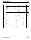
t13
Read Command Hold (REG[22h] bit 4 = 0 and bits 3-
2 = 00)
4 t1 - 3 ns
Read Command Hold (REG[22h] bit 4 = 0 and bits 3-
2 = 01 or 10)
3 t1 - 3 ns
Read Command Hold (REG[22h] bit 4 = 1 and bits 3-
2 = 00)
3 t1 - 3 ns
Read Command Hold (REG[22h] bit 4 = 1 and bits 3-
2 = 01 or 10)
2 t1 - 3 ns
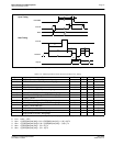
t14 Read Data Setup referenced from CAS# 5 ns
t15 Bus Tri-State 3 t1- 5 ns
t16 Write Command Setup 0.45 t1- 3 ns
t17 Write Command Hold 0.45 t1 - 3 ns
t18 Write Data Setup 0.45 t1 - 3 ns
t19 Write Data Hold 0.45 t1 - 3 ns
t20 MD Tri-state 0.45 t1 0.45t1 + 21 ns
t21 CAS# to WE# active during Read-Write cycle 0.45 t1 - 3 ns
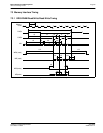
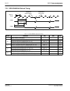
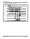
Table 7-18: FPM-DRAM Read/Write/Read-Write Timing
Symbol Parameter Min Max Units