


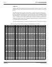
Page 32
Epson Research and Development
Vancouver Design Center
S1D13505 Programming Notes and Examples
X23A-G-003-07 Issue Date: 01/02/05
Both panning and scrolling are performed by modifying the start address register. The start
address refers to the word offset in the display buffer where the image will start being
displayed from. At color depths less than 15 bpp a second register, the pixel pan register, is
required for smooth pixel level panning.
Internally, the S1D13505 latches different signals at different times. Due to this internal
sequence, there is an order in which the start address and pixel pan registers should be
accessed during scrolling operations to provide the smoothest scrolling. Setting the
registers in the wrong sequence or at the wrong time will result in a “tearing” or jitter effect
on the display.
The start address is latched at the beginning of each frame, therefore the start address can
be set any time during the display period. The pixel pan register values are latched at the
beginning of each display line and must be set during the vertical non-display period. The
correct sequence for programing these registers is:
1. Wait until just after a vertical non-display period (read register [0Ah] and watch bit 7
for the non-display status).
2. Update the start address registers.
3. Wait until the next vertical non-display period.
4. Update the pixel paning register.
5.2.1 Registers
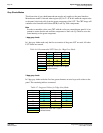
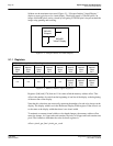
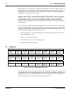
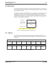
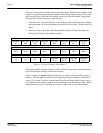
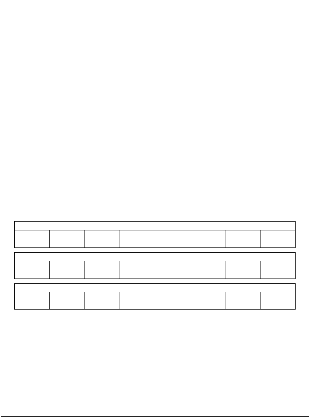
Figure 5-3: Screen 1 Start Address Registers
These three registers form the address of the word in the display buffer where screen 1 will
start displaying from. Changing these registers by one will cause a change of 0 to 16 pixels
depending on the current color depth. Refer to the following table to see the minimum
number of pixels affected by a change of one to these registers.
REG[10h] Screen 1 Display Start Address 0
Start Addr
Bit 7
Start Addr
Bit 6
Start Addr
Bit 5
Start Addr
Bit 4
Start Addr
Bit 3
Start Addr
Bit 2
Start Addr
Bit 1
Start Addr
Bit 0
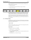
REG[11h] Screen 1 Display Start Address 1
Start Addr
Bit 15
Start Addr
Bit 14
Start Addr
Bit 13
Start Addr
Bit 12
Start Addr
Bit 11
Start Addr
Bit 10
Start Addr
Bit 9
Start Addr
Bit 8
REG[12h] Screen 1 Display Start Address 2
n/a n/a n/a n/a
Start Addr
Bit 19
Start Addr
Bit 18
Start Addr
Bit 17
Start Addr
Bit 16