


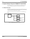

Page 10
Epson Research and Development
Vancouver Design Center
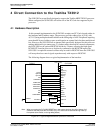
S1D13505 Interfacing to the Toshiba MIPS TX3912 Processor
X23A-G-010-04 Issue Date: 01/02/05
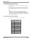
3.2 TX3912 Host Bus Interface Signals
When the S1D13505 is configured to operate with the TX3912, the host interface requires
the following signals:
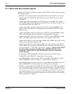
• BUSCLK is a clock input required by the S1D13505 host bus interface. It is separate
from the input clock (CLKI) and should be driven by the TX3912 bus clock output
DCLKOUT.
• Address input AB20 corresponds to the TX3912 signal ALE (address latch enable)
whose falling edge indicates that the most significant bits of the address are present on
the multiplexed address bus (AB[12:0]).
• Address input AB19 should be connected to the TX3912 signal CARDREG*. This
signal is active when either IO or configuration space of the TX3912 PC Card slot is
being accessed.
• Address input AB18 should be connected to the TX3912 signal CARDIORD*. Either
AB18 or the RD# input must be asserted for a read operation to take place.
• Address input AB17 should be connected to the TX3912 signal CARDIOWR*. Either
AB17 or the WE0# input must be asserted for a write operation to take place.
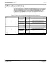
• Address inputs AB[16:13] and control inputs M/R#, CS# and BS# must be tied to V
DD
as they are not used in this interface mode.
• Address inputs AB[12:0], and the data bus DB[15:0], connect directly to the TX3912
address and data bus, respectively. MD4 must be set to select the proper endian mode on
reset (see Section 4.2, “S1D13505 Configuration” on page 12). Because of the TX3912
data bus naming convention and endian mode, S1D13505 DB[15:8] must be
connected to TX3912 D[23:16], and S1D13505 DB[7:0] must be connected to
TX3912 D[31:24].
• Control inputs WE1# and RD/WR# should be connected to the TX3912 signals
CARDxCSH* and CARDxCSL* respectively for byte steering.
• Input RD# should be connected to the TX3912 signal RD*. Either RD# or the AB18
input (CARDIORD*) must be asserted for a read operation to take place.
• Input WE0# should be connected to the TX3912 signal WR*. Either WE0# or the AB17
input (CARDIOWR*) must be asserted for a write operation to take place.
• WAIT# is a signal output from the S1D13505 that indicates the TX3912 must wait until
data is ready (read cycle) or accepted (write cycle) on the host bus. Since the TX3912
accesses to the S1D13505 may occur asynchronously to the display update, it is possible
that contention may occur in accessing the S1D13505 internal registers and/or display
buffer. The WAIT# line resolves these contentions by forcing the host to wait until the
resource arbitration is complete.