


Epson Research and Development
Page 99
Vancouver Design Center
Hardware Functional Specification S1D13505
Issue Date: 01/02/02 X23A-A-001-14
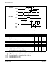
8 Registers
8.1 Register Mapping
The S1D13505 registers are memory mapped. The system addresses the registers through the CS#,
M/R#, and AB[5:0] input pins. When CS# = 0 and M/R# = 0, the registers are mapped by address
bits AB[5:0], e.g. REG[00h] is mapped to AB[5:0] = 000000, REG[01h] is mapped to AB[5:0] =
000001. See the table below:
8.2 Register Descriptions
Unless specified otherwise, all register bits are reset to 0 during power-on. Reserved bits should be
written 0 when programming unless otherwise noted.
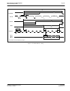
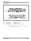
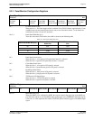
8.2.1 Revision Code Register
bits 7-2 Product Code Bits [5:0]
This is a read-only register that indicates the product code of the chip. The product code for the
S1D13505 is 000011.
bits 1-0 Revision Code Bits [1:0]
This is a read-only register that indicates the revision code of the chip. The revision code for the
S1D13505F00A is 00.
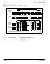
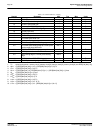
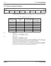
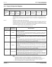
Table 8-1: S1D13505 Addressing
CS# M/R# Access
00
Register access:
• REG[00h] is addressed when AB[5:0] = 0
• REG[01h] is addressed when AB[5:0] = 1
• REG[n] is addressed when AB[5:0] = n
01
Memory access: the 2M byte Display Buffer is addressed by
AB[20:0]
1X
S1D13505 not selected
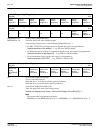
Revision Code Register
REG[00h] RO
Product Code
Bit 5
Product Code
Bit 4
Product Code
Bit 3
Product Code
Bit 2
Product Code
Bit 1
Product Code
Bit 0
Revision
Code Bit 1
Revision
Code Bit 0