


Epson Research and Development
Page 59
Vancouver Design Center
Hardware Functional Specification S1D13505
Issue Date: 01/02/02 X23A-A-001-14
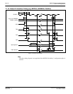
1. If the S1D13505 host interface is disabled, the timing for CARDxWAIT* driven is relative to
the falling edge of chip select or
the second positive edge of DCLKOUT after ADDR[12:0]
becomes valid, whichever one is later.
2. If the S1D13505 host interface is disabled, the timing for D[31:16] driven is relative to the
falling edge of chip select or
the second positive edge of DCLKOUT after ADDR[12:0] be-
comes valid, whichever one is later.
Note
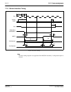
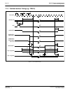
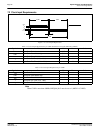
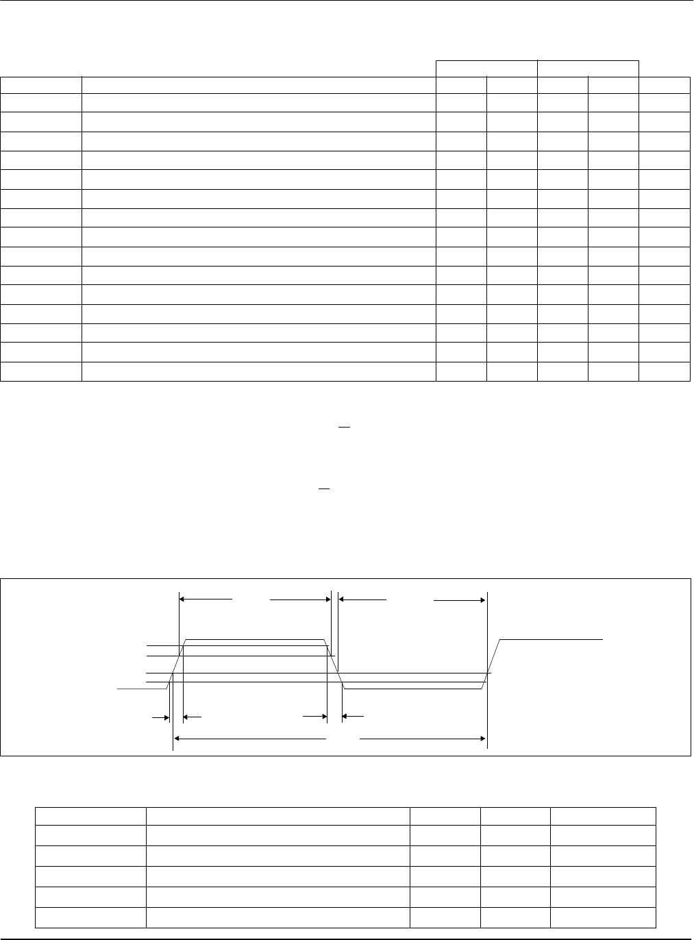
The Toshiba interface has different clock input requirements as follows:
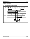
Figure 7-11: Clock Input Requirement
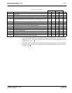
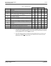
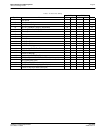
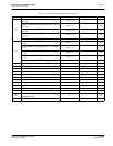
Table 7-10: Toshiba Timing
3.0V 5.0V
Symbol Parameter Min Max Min Max Units
t1
Clock period
13.3 13.3 ns
t2
Clock pulse width low
5.4 5.4 ns
t3
Clock pulse width high
5.4 5.4 ns
t4
ADDR[12:0] setup to first CLK of cycle
10 10 ns
t5
ADDR[12:0] hold from command invalid
00ns
t6
ADDR[12:0] setup to falling edge ALE
10 10 ns
t7
ADDR[12:0] hold from falling edge ALE
55ns
t8
CARDREG* hold from command invalid
00ns
t9
1
Falling edge of chip select to CARDxWAIT* driven
0150 9ns
t10
Command invalid to CARDxWAIT* tri-state
5 25 2.5 10 ns
t11
D[31:16] valid to first CLK of cycle (write cycle)
10 10 ns
t12
D[31:16] hold from rising edge of CARDxWAIT*
00
t13
2
Chip select to D[31:16] driven (read cycle)
11ns
t14
D[31:16] setup to rising edge CARDxWAIT* (read cycle)
00ns
t15
Command invalid to D[31:16] tri-state (read cycle)
5 25 2.5 10 ns
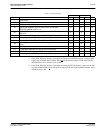
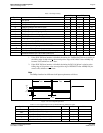
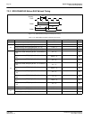
Table 7-11: Clock Input Requirements for BUSCLK using Toshiba local bus
Symbol Parameter Min Max Units
T
OSC
Input Clock Period)
13.3 ns
t
PWH
Input Clock Pulse Width High
5.4 ns
t
PWL
Input Clock Pulse Width Low
5.4 ns
t
f
Input Clock Fall Time (10% - 90%)
5ns
t
r
Input Clock Rise Time (10% - 90%)
5ns
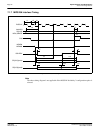
t
PWL
t
PWH
t
f
t
r
T
OSC
V
IH
V
IL
10%
90%