Intel® PXA255 Processor Developer’s Manual 4-1
System Integration Unit 4
This chapter describes the System Integration Unit (SIU) for the PXA255 processor. The SIU
controls several processor-wide system functions. The units contained in the SIU are:
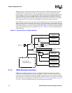
• General-purpose I/O (GPIO) ports
• Interrupt controller
• Real-time clock (RTC)
• Operating system timer (OS timer)
• Pulse Width modulator
4.1 General-Purpose I/O
The PXA255 processor enables and controls its 81 GPIO pins through the use of 27 registers which
configure the pin direction (input or output), pin function, pin state (outputs only), pin level
detection (inputs only), and selection of alternate functions. A portion of the GPIOs can be used to
bring the processor out of Sleep mode. Take care when choosing which GPIO pin is assigned as a
GPIO function because many of the GPIO pins have alternate functions and can be configured to
support processor peripherals.
Configure all unused GPIOs as outputs to minimize power consumption.
4.1.1 GPIO Operation
The PXA255 processor provides 81 GPIO pins for use in generating and capturing application-
specific input and output signals. Each pin can be programmed as either an input or output. When
programmed to be an input, a GPIO can also serve as an interrupt source. All 81 pins are
configured as inputs during the assertion of all resets, and remain as inputs until they are
configured otherwise.
Use the GPIO Pin Direction Register (GPDR) to set whether the GPIO pins are outputs or inputs.
When programmed as an output, the pin can be set high by writing to the GPIO Pin Output Set
Register (GPSR) and cleared low by writing to the GPIO Pin Output Clear Register (GPCR). The
set and clear registers can be written to regardless of whether the pin is configured as an input or an
output. If a pin is configured as an input, the programmed output state occurs when the pin is
reconfigured to be an output.
Validate each GPIO pin’s state by reading the GPIO Pin Level Register (GPLR). You can read this
register any time to confirm the state of a pin. In addition, use the GPIO Rising Edge Detect Enable
Register (GRER) and GPIO Falling Edge Detect Enable Register (GFER) to detect either a rising
edge or falling edge on each GPIO pin. Use the GPIO Edge Detect Status register (GEDR) to read
edge detect state. These edge detects can be programmed to generate interrupts (see Section 4.2).
Also use GPIO[15:0] to generate wake-up events that bring the PXA255 processor out of sleep
mode (refer to Section 3.4.9.5, “Exiting Sleep Mode” on page 3-18).


