6-18 Intel® PXA255 Processor Developer’s Manual
Memory Controller
6.5.5 SDRAM Memory Options
The Dynamic Memory interface supports up to four partitions, organized as two pairs. Both
partitions in a pair must have the same SDRAM size, configuration, timing category, and data bus
width. Initialization software must set up the memory interface configuration register with:
• SDRAM timing category
• Data-bus width
• Number of row, column, and bank address bits
• Addressing scheme
• Data-latching scheme
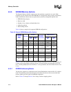
Table 6-6 shows a sample of the supported SDRAM configurations.
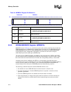
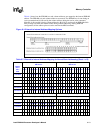
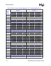
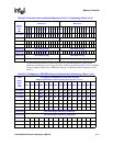
Figure 6-4 shows the bank/row/column address multiplexing using a 2x13x9 32-bit SDRAM as an
example for the normal bank-addressing scheme.
All unused address bits during RAS and CAS
time - including MA[9:0] bits not shown here - are not guaranteed, and will be either driven to zero
or one.
6.5.5.1 SDRAM Addressing Modes
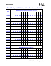
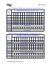
The processor supports two addressing modes: Normal Bank Address mode and SA-1111 Address
mode. The addressing mode alters the order of the address bits that are driven on the individual
memory address pins and control the SDRAM components.
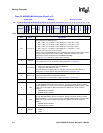
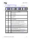
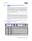
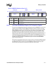
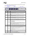
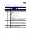
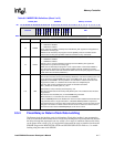
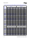
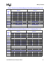
Refer to Table 6-7 through Table 6-9 for a listing of address mapping options.
Table 6-6. Sample SDRAM Memory Size Options
SDRAM
Configuration
(Words x
Bits)
Chip Size
Number Chips/
Partition
Bank Bits x
Row Bits x
Column Bits
Partition Size
(Mbyte/Partition)
16-Bit
Bus
32-Bit
bus
16-Bit
Bus
32-Bit
Bus
1M x 16 16 Mbit 1 2 1 x 11 x 8 2 Mbyte 4 Mbyte
2 M x 8 16 Mbit 2 4 1 x 11 x 9 4 Mbyte 8 Mbyte
2 M x 32 64 Mbit N/A 1 2 x 11 x 8 N/A 8 Mbyte
4 M x 16 64 Mbit 1 2
1 x 13 x 8
2 x 12 x 8
8 Mbyte 16 Mbyte
8 M x 8 64 Mbit 2 4
1 x 13 x 9
2 x 12 x 9
16 Mbyte 32 Mbyte
8 M x 16 128 Mbit 1 2 2 x 12 x 9 16 Mbyte 32 Mbyte
16 M x 8 128 Mbit 2 4 2 x 12 x 10 32 Mbyte 64 Mbyte
16 M x 16 256 Mbit 1 2 2 x 13 x 9 32 Mbyte 64 Mbyte
32 M x 8 256 Mbit 2 4 2 x 13 x 10 64 Mbyte
128 Mbyte -
exceeds
partition size


