Intel® PXA255 Processor Developer’s Manual 13-7
AC’97 Controller Unit
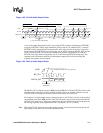
Only one I/O cycle can be pending across the AC-link at any time. The ACUNIT uses write and
read posting on I/O accesses across the link. For example, read data from a CODEC register is not
sent over the AC-link (Slot 2 of incoming stream) within the same frame that the read request is
sent.
For CODEC reads, the ACUNIT gives the CODEC a maximum of four subsequent frames to
respond -- if no response is received, the ACUNIT returns a dummy read completion
(0xFFFF_FFFF) to the CPU and sets the Read Completion Status (RDCS) bit of the Global Status
Register (GSR).
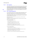
The CAIP bit of the CODEC Access Register (CAR) is used to assure that only one I/O cycle
occurs across the AC-link at any time. Software must read the CAIP bit before initiating an I/O
cycle. If the CAIP bit reads as a one, another driver is performing an I/O cycle; if the CAIP bit
reads as a zero, a new I/O cycle can be initiated.
The exception to posted accesses is reads to the CODEC GPIO Pin Status register (address 0x54).
CODEC GPIO Pin Status read data is sent by the CODEC over the AC-link in the same frame that
the read request was sent to the CODEC. The CODEC GPIO Pin Status read data is sent in Slot 12
of the incoming stream. A CODEC with a GPIO Pin Status register must constantly send the status
of the register in slot 12.
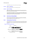
13.4.1.3 Slot 2: Command Data Port
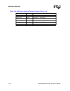
Slot 2 is the Command Data Port. Slot 2 (in conjunction with the Command Address Port of Slot 1)
delivers 16-bit control register write data in the event that the current command port operation is a
write cycle (as indicated by slot 1, bit 19).
If the current command port operation is a read, the ACUNIT fills Slot 2 with zeroes.
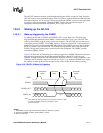
13.4.1.4 Slot 3: PCM Playback Left Channel
Slot 3 contains the composite digital audio left playback stream. If the playback stream contains an
audio sample with a resolution that is less than 20 bits, the ACUNIT fills all trailing non-valid bit
positions with zeroes.
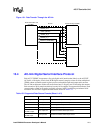
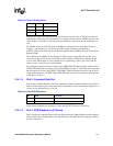
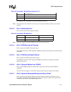
Table 13-3. Slot 1 Bit Definitions
Bit Name Description
Bit(19) RW 1 = read, 0 = write
Bit(18:12) IDX Code register index
Bit(11:0) reserved Stuff with 0s
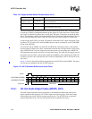
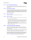
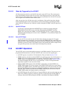
Table 13-4. Slot 2 Bit Definitions
Bit Name Description
Bit(19:4) Control register write data Stuffed with 0s if current operation is a read
Bit(3:0) reserved Stuffed with 0s


