11-8 Intel® PXA255 Processor Developer’s Manual
Fast Infrared Communication Port
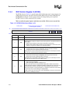
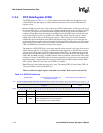
11.3.1 FICP Control Register 0 (ICCR0)
The ICCR0, shown in Table 11-2, contains eight valid bit fields that control various functions for
4 Mbps IrDA transmission. The FICP must be disabled (RXE=TXE=0) when ICCR0[ITR] and
ICCR0[LBM] are changed. To allow various modes to be changed during active operation,
ICCR0[7:2] may be written when the FICP is enabled.
This is a read/write register. Ignore reads from reserved bits. Write zeros to reserved bits.
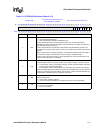
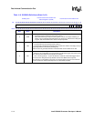
Table 11-2. ICCR0 Bit Definitions (Sheet 1 of 2)
0x4080_0000
Fast Infrared Communication Port
Control Register 0 (ICCR0)
Fast Infrared Communication Port
Bit
31 30 29 28 27 26 25 24 23 22 21 20 19 18 17 16 15 14 13 12 11 10 9 8 7 6 5 4 3 2 1 0
reserved
AME
TIE
RIE
RXE
TXE
TUS
LBM
ITR
Reset 0 0 0 0 0 0 0 0 0 0 0 0 0 0 0 0 0 0 0 0 0 0 0 0 0 0 0 0 0 0 0 0
Bits Name Description
[31:8] — reserved
7AME
Address match enable.
Receive logic will compare the address of the incoming frames to the Address Match Value
field in ICCR1.
0 = Disable receiver address match function. Store data in receive FIFO.
1 = Enable receiver address match function. Do not put data in the receive FIFO unless
address is recognized or address is the broadcast address.
6TIE
Transmit FIFO interrupt enable.
0 = Transmit FIFO service request, ICSR0[TFS], does not generate an interrupt.
1 = Transmit FIFO service request generates an interrupt.
Setting TIE does not clear TFS or prevent TFS from being set or cleared by the transmit
FIFO. TIE does not affect transmit FIFO DMA requests.
5RIE
Receive FIFO interrupt enable.
0 = Receive FIFO service request, ICSR0[RFS], does not generate an interrupt.
1 = Receive FIFO service request generates an interrupt
Setting RIE does not clear RFS or prevent RFS from being set or cleared by the receive
FIFO. RIE does not affect receive FIFO DMA requests.
4RXE
Receive enable.
0 = FICP receive logic disabled.
1 = FICP receive logic enabled if ICCR0[ITR] is set.
All other control bits must be configured before setting RXE. If RXE is cleared while
receiving data then reception is stopped immediately, all data within the receive FIFO and
serial input shifter is cleared, and control of the receive data pin is given to the SIU.
While communication is normally half-duplex, it is possible to transmit and receive data at
the same time. This is used for testing in Loopback Mode.
If RXE is used to clear the receive FIFO, check ICSR1[RNE] to ensure the receive FIFO is
clear before re-enabling the receiver.


