6-8 Intel® PXA255 Processor Developer’s Manual
Memory Controller
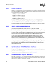
6.4.1 Reads and Writes
DQM[3:0] are data masking bits. When asserted (high), the corresponding bit masks the associated
byte of data on the MD[31:0] bus. When deasserted (low), the corresponding bit does not mask the
associated byte of data on the MD[31:0] bus.
• DQM[3] corresponds to MD[31:24]
• DQM[2] corresponds to MD[23:16]
• DQM[1] corresponds to MD[15:8]
• DQM[0] corresponds to MD[7:0]
For writes to SDRAM, SRAM, or Variable Latency I/O memory spaces, the DQM[3:0] lines
enable the corresponding byte of the data bus. Flash memory space stores must be exactly the
width of the Flash data bus, either 16- or 32-bits. See Section 6.7.6 for more information.
For reads to all memory types, the DQM[3:0] lines are deasserted (set low so data is not masked).
6.4.2 Aborts and Nonexistent Memory
Accessing reserved portions of the memory map results in a data abort exception.
Hardware does not detect reads and writes from or to enabled and nonexistent memory. If memory
in an enabled partition is not present, a read returns indeterminate data.
If memory does not occupy all 64 MB of the partition, reads and writes from or to the unoccupied
portion are processed as if the memory occupies the entire 64 MB of the memory partition.
A single word (or half-word if the data bus width is defined as 16-bits) access to a disabled
SDRAM partition (MDCNFG:DEx=0) causes a CBR refresh cycle to all four partitions. This
technique is used in the hardware initialization procedure. Read return data is indeterminate and
writes are not executed on the external memory bus.
A burst read access to a disabled SDRAM partition results in a target-abort exception. Target aborts
are also generated for burst writes to Flash/ROM space and bursts to configuration space.
Attempted single beat writes to ROM are not aborted. Bursts to configuration space also result in
target aborts. Target aborts can be either Data or Prefetch abort depending on the source of the
attempted burst transaction.
6.5 Synchronous DRAM Memory Interface
Each possible SDRAM portion of the Memory Map is referred to as a partition, to distinguish them
from banks internal to SDRAM devices.
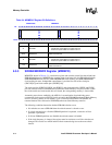
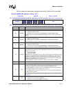
The signals used to control the SDRAM memory are listed in Section 6.2.1.
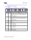
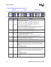
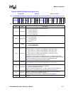
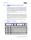
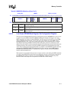
6.5.1 SDRAM MDCNFG Register (MDCNFG
MDCNFG, shown in Table 6-2, is a read/write register and contains control bits for configuring the
SDRAM. Both SDRAM partitions in a pair (0/1 or 2/3) must be implemented with the same type of
SDRAM devices, but the two partition pairs may differ.


