


12-10 Intel® PXA255 Processor Developer’s Manual
USB Device Controller
The direction of the endpoints is fixed. Physically, the UDC only supports interrupt endpoints with
a maximum packet size of 8 bytes or less, bulk endpoints with a maximum packet size of 64 bytes
or less, and isochronous endpoints with a maximum packet size of 256 bytes or less.
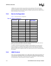
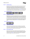
To make the processor more adaptable, the UDC supports a total of four configurations. Each of
these configurations are identical in the UDC, software can make three distinct configurations,
each with two interfaces. Configuration 0 is a default configuration of Endpoint 0 only and cannot
be defined as any other arrangement.
After the host completes a SET_CONFIGURATION or SET_INTERFACE command, the
software must decode the command to empty the OUT endpoint FIFOs and allow the Megacell to
set up the proper power/peripheral configurations.
12.4 UDC Hardware Connection
This section explains how to connect the USB interface for a variety of devices.
12.4.1 Self-Powered Device
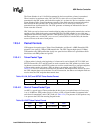
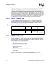
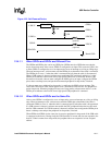
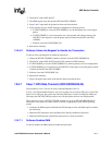
Figure 12-2 shows how to connect the USB interface for a self-powered device. The 0 Ω resistors
are optional and if they are not used, USB D+ must connect directly to the device UDC D+ and
connect USB D- must connect directly to the device UDC D-. The UDC D+ and UDC D- pins are
designed to match the impedance of a USB cable, 90
Ω, without external series resistors. To allow
minor impedance corrections to compensate for the impedance that results from the board trace,
0
Ω resistors are recommended on the board.
The “5 V to 3.3 V” device is required because the input pins of the processor can only tolerate 3.3
V. The device can be implemented in a number of ways. The most robust and expensive solution is
a Power-On-Reset device such as a MAX6348. This solution produces a clean signal edge and
minimizes signal bounce. A more inexpensive solution is a 3.3 V line buffer with inputs that can
tolerate 5 V. This solution does not reduce signal bounce, so software must compensate by reading
the GPIO repeatedly until it proves to be stable. A third solution is a signal bounce minimization
circuit that can tolerate 5 V but produces a 3.3 V signal to the GPIO pin.