11-4 Intel® PXA255 Processor Developer’s Manual
Fast Infrared Communication Port
11.2.6 CRC Field
The FICP uses a 32-bit Cyclic Redundancy Check (CRC) to detect bit errors that occur during
transmission. The CRC is generated from the address, control, and data fields, and is included in
each frame. Transmit and receive logic have separate CRC generators. The CRC computation logic
is set to all ones before each frame is transmitted or received and the result is inverted before it is
used for comparison or transmission. The transmitter calculates a CRC as data is transmitted and
places the inverse of the resulting 32-bit value at the end of each frame until the stop flag is
transmitted. The receiver also calculates a CRC and inverts it for each data frame that it receives.
The receiver compares the calculated CRC to the expected CRC value at the end of each frame.
If the calculated value does not match the expected value, the CRC error bit that corresponds to the
last data byte received is set. When this byte reaches the trigger level range, an interrupt is
generated.
Note: Unlike the address, control, and data fields, the 32-bit inverted CRC value is transmitted and
received most significant nibble first.
The cyclic redundancy checker uses the 32-term polynomial:
11.2.7 Baud Rate Generation
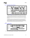
The baud rate is derived by dividing a fixed 48-MHz clock by six. Using a digital PLL, the 8-MHz
baud (or timeslot) clock for the receive logic is synchronized with the 4PPM data stream each time
a transition is detected on the receive data line. To encode a 4-Mbps data stream, the required chip
frequency is 2.0 MHz, with four timeslots per chip at a frequency of 8.0 MHz. Receive data is
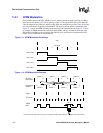
sampled halfway through each timeslot period by counting three of the six 48-MHz clock periods
that make up each timeslot (see Figure 11-2). The chips are synchronized during the reception
preamble. The pattern of four chips repeated 16 times is used to identify the first timeslot (or the
beginning of a chip) and resets the 2-bit timeslot counter logic.
11.2.8 Receive Operation
The IrDA standard specifies that all transmission occurs at half-duplex. This restriction forces
software to enable one direction at a given time. Either the transmit or receive logic can be enabled,
but not both. The FICP’s hardware does not impose such a restriction.The software can enable both
the transmitter and receiver. This feature is used with the FICP’s loopback mode, which internally
connects the output of the transmit serial shifter to the input of the receive serial shifter.
After the FICP is enabled, the receiver logic begins and selects an arbitrary chip boundary, uses a
serial shifter to receive four incoming 4PPM chips from the receive data pin, and latches and
decodes the chips one at a time. If the chips do not have the correct preamble, the timeslot
counter’s clock skips one 8-MHz period and effectively delays the timeslot count by one. This
process is called hunt mode and is repeated until the chips have the correct preamble, which
indicates that the timeslot counter is synchronized. The preamble can be repeated as few as 16
times or can be continuously repeated to indicate an idle transmit line.
CRC x() x
32
x
26
x
23
x
22
x
16
x
12
x
11
x
10
x
8
x
7
x
5
x
4
x
2
x 1+ + + + + + + +++++++( )=


