


4-16 Intel® PXA255 Processor Developer’s Manual
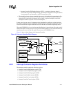
System Integration Unit
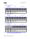
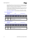
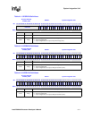
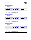
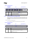
4.1.3.6 GPIO Alternate Function Register (GAFR0_L, GAFR0_U, GAFR1_L,
GAFR1_U, GAFR2_L, GAFR2_U)
GAFR0_L, GAFR0_U, GAFR1_L, GAFR1_U, GAFR2_L, GAFR2_U, shown in Table 4-24,
Table 4-25, Table 4-26, Table 4-27, Table 4-28, and Table 4-29, contain select bits that correspond
to the 81 GPIO pins. Each GPIO can be configured to be either a generic GPIO pin, one of 3
alternate input functions, or one of 3 alternate output functions. To select any of the alternate
functions, the GPDR register must configure the GPIO to be an input. Similarly, only GPIOs
configured as outputs by the GPDR can be configured for alternate output functions. Each GPIO
pin has a pair of bits assigned to it whose values determine which function (normal GPIO, alternate
function 1, alternate function 2 or alternate function 3) the GPIO performs. The function selected is
determined by writing the GAFR bit pair as below:
• “00” indicates normal GPIO function
• “01” selects alternate input function 1 (ALT_FN_1_IN) or alternate output function 1
(ALT_FN_1_OUT)
• “10” selects alternate input function 2 (ALT_FN_2_IN) or alternate output function 2
(ALT_FN_2_OUT)
• “11” selects alternate input function 3 (ALT_FN_3_IN) or alternate output function 3
(ALT_FN_3_OUT)
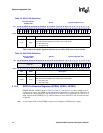
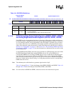
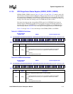
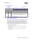
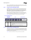
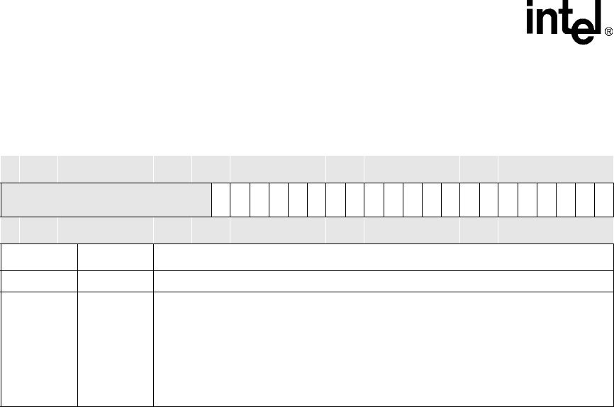
Table 4-23. GEDR2 Bit Definitions
Physical Address
0x40E0_0050
GEDR2 System Integration Unit
Bit
31 30 29 28 27 26 25 24 23 22 21 20 19 18 17 16 15 14 13 12 11 10 9 8 7 6 5 4 3 2 1 0
reserved
ED84
ED83
ED82
ED81
ED80
ED79
ED78
ED77
ED76
ED75
ED74
ED73
ED72
ED71
ED70
ED69
ED68
ED67
ED66
ED65
ED64
Reset 0 0 0 0 0 0 0 0 0 0 0 0 0 0 0 0 0 0 0 0 0 0 0 0 0 0 0 0 0 0 0 0
Bits Name Description
<31:21> — reserved
<20:0> ED[x]
GPIO Pin ‘x’ Edge Detect Status (where x=64 through 80).
READ
0 – No edge detect has occurred on pin as specified in GRER and/or GFER.
1 – Edge detect has occurred on pin as specified in GRER and/or GFER.
WRITE
0 – No effect.
1 – Clear edge detect status field.