


Intel® PXA255 Processor Developer’s Manual 6-19
Memory Controller
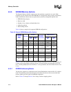
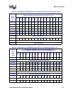
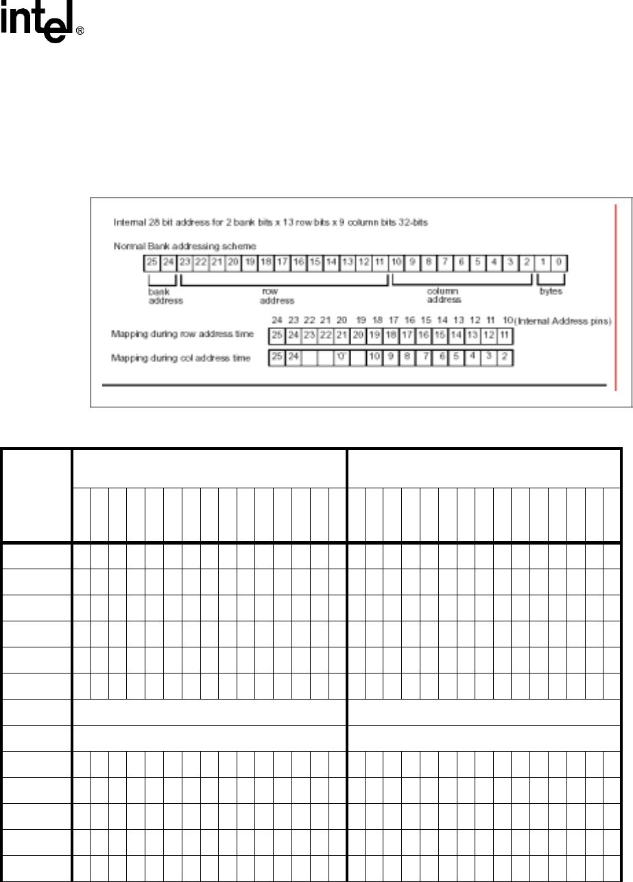
Table 6-4 shows how the SDRAM row and column addresses are mapped to the internal SDRAM
address. The SDRAM row and column addresses are muxed. The SDRAM row is sent during an
Active command and is followed by the column address during the read or write command.
MA<20> is driven with 0 during column addressing. BA[1:0] is used to tell the SDRAM which
bank is being read from and remains stable during column addressing. During SDRAM
configuration, all the address pins are used to transfer the MRS command.
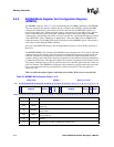
Figure 6-4. External to Internal Address Mapping Options
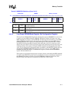
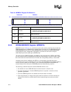
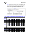
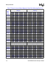
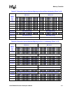
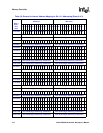
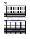
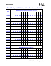
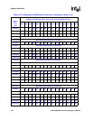
Table 6-7. External to Internal Address Mapping for Normal Bank Addressing (Sheet 1 of 3)
# Bits
Bank x
Row x
Col x
Data
External Address pins at SDRAM RAS Time
MA<24:10>
External Address pins at SDRAM CAS Time
MA<24:10>
24 23 22 21 20 19 18 17 16 15 14 13 12 11 10 24 23 22 21 20 19 18 17 16 15 14 13 12 11 10
1x11x8x32 21 20 19 18 17 16 15 14 13 12 11 10 21 ‘0’ 9 8765432
1x11x8x16 20 19 18 17 16 15 14 13 12 11 10 9 20 ‘0’ 8 7654321
1x11x9x32 22 21 20 19 18 17 16 15 14 13 12 11 22 ‘0’ 10 9 8765432
1x11x9x16 21 20 19 18 17 16 15 14 13 12 11 10 21 ‘0’ 9 8 7654321
1x11x10x32 232221201918171615141312 23‘0’111098765432
1x11x10x16 222120191817161514131211 22‘0’10987654321
1x11x11x32 NOT VALID (illegal addressing combination) NOT VALID (illegal addressing combination)
1x11x11x16 NOT VALID (illegal addressing combination) NOT VALID (illegal addressing combination)
1x12x8x32 22212019181716151413121110 22 ‘0’ 98765432
1x12x8x16 2120191817161514131211109 21 ‘0’ 87654321
1x12x9x32 23222120191817161514131211 23 ‘0’ 1098765432
1x12x9x16 22212019181716151413121110 22 ‘0’ 987654321
1x12x10x32 24 23 22 21 20 19 18 17 16 15 14 13 12 24 ‘0’ 11 10 9 8765432