6-70 Intel® PXA255 Processor Developer’s Manual
Memory Controller
6.9.1 Alternate Bus Master Mode
The processor supports the presence of an alternate master on the SDRAM memory bus. The
alternate master is given control of the bus with a hardware handshake that is performed through
MBREQ and MBGNT, which are invoked through the alternate functions on GPIO[14] and
GPIO[13], respectively. The Memory Controller performs an SDRAM refresh if SDRAM clocks
and clock enable are turned on. When the alternate master must take control of the memory bus, it
asserts MBREQ. It then deasserts SDCKE<1> and three-states all memory bus pins used with
SDRAM bank 0 (nSDCS<0>, MA[25:0], nOE, nWE, nSDRAS, nSDCAS, SDCLK<1>,
MD[31:0], DQM[3:0]). All other memory and 16-bit PC Card pins remain driven. RD/nWR
remain low. Then the processor asserts MBGNT, the alternate master starts to drive all pins
including SDCLK<1>, and the processor reasserts SDCKE<1>.
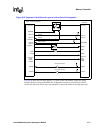
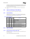
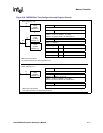
The grant sequence and timing follow:
1. The Alternate master asserts MBREQ.
2. The Memory Controller performs an SDRAM refresh if SDRAM clocks and clock enable are
turned on
3. If the MDCNFG:SA1111x bit is enabled, the Memory Controller sends the SDRAMs an MRS
command to change the SDRAM burst length to one. The burst length is changed to one for
SA-1111 compatibility.
4. The processor deasserts SDCKE<1> at time (t).
5. The processor three-states SDRAM outputs at time (t + 1 MEMCLK).
6. The processor asserts MBGNT at time (t + 2 MEMCLKS).
7. The Alternate master drives SDRAM outputs before time (t + 3 MEMCLKS).
8. The processor asserts SDCKE<1> at time (t + 4 MEMCLKS).
During the three-state period, both MBREQ and MBGNT remain high and an external device can
take control of the three-stated pins. The external device must drive all the three-stated pins.
Floating inputs can cause excessive crossover current and erroneous SDRAM commands. During
the three-state period, the processor can not perform SDRAM refresh cycles.
The alternate master must assume the responsibility for SDRAM integrity during the three-state
period. The system must be designed to ensure that the period of alternate mastership is limited to
less than the refresh period or that the alternate master implements a refresh counter to perform
refreshes at the proper intervals.
To surrender the bus, the alternate master deasserts MBREQ. The processor deasserts SDCKE<1>
and MBGNT. The alternate master stops driving the SDRAM pins. The processor drives all
SDRAM pins and then re-asserts SDCKE<1>.
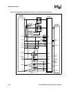
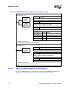
The release sequence and timing follows:
1. The Alternate master deasserts MBREQ.
2. The processor deasserts SDCKE<1> at time (t).
3. The processor deasserts MBGNT at time (t + 1 MEMCLK).
4. The Alternate master three-states SDRAM outputs prior to time (t + 2 MEMCLKS).
5. The processor drives SDRAM outputs at time (t + 3 MEMCLKS).
6. The processor asserts SDCKE<1> at time (t + 4 MEMCLKS).


