14-8 Intel® PXA255 Processor Developer’s Manual
Inter-Integrated-Circuit Sound (I2S) Controller
14.6 Registers
The I
2
S Controller registers are all 32-bit addressable, ranging from 0x4040_0000 through
0x404F_FFFF.
The I
2
S Controller has the following types of registers:
• Control registers are used to program common control, alternate mode specific control.
• The Data Register is used for Transmit and Receive FIFO accesses.
• The Status Register signals the state of the FIFO buffers and the status of the interface that is
selected by the common control register.
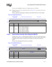
• The Interrupt Registers include the Interrupt Mask Register, the Interrupt Clear Register, and
the Interrupt Test Register.
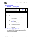
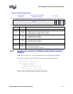
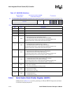
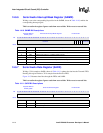
14.6.1 Serial Audio Controller Global Control Register (SACR0)
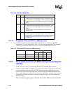
SACR0, shown in Table 14-3, controls common I
2
S functions.
The ENB bit controls the I2SLINK, as follows:
• Clearing ENB to zero does the following:
— disables any I2SLINK activity
— resets all Receive FIFO pointers and also the counter that controls the I2SLINK
— resets the Receive FIFO
— does not affect the Transmit FIFO
— the output pin SYNC will not toggle
— de-asserts all DMA requests
— any read accesses to the Data Register (SADR), by the processor, or by the DMA
controller is returned with zeros
— disables all interrupts.
• Setting ENB to one does the following:
— enables I2SLINK activity
— enables DMA requests.
Note: If ENB is toggled in the middle of a normal operation, the RST bit must also be set and cleared to
reset all I2SC registers.
Note: The SACR0[ENB] control signal crosses clock domains. It is registered in an internal clock
domain that is much faster than the BITCLK domain. It takes four BITCLK cycles and four
internal clock cycles before SACR0[ENB] is conveyed to the slower BITCLK domain. If the
control setting is modified at a rate faster than (4 BITCLK + 4 internal clock) cycles, the last
updated value in this time frame is stored in a temporary register and is transferred to the BITCLK
domain.
This is a read/write register. Ignore reads from reserved bits. Write zeros to reserved bits.


