


17-18 Intel® PXA255 Processor Developer’s Manual
Hardware UART
This is a read-only register. Ignore reads from reserved bits.
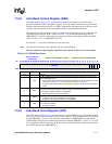
17.5.10 Line Control Register (LCR)
The LCR., shown in Table 17-14 specifies the format for the asynchronous data communications
exchange. The serial data format consists of a start bit, five to eight data bits, an optional parity bit,
and one, one and a half, or two stop bits. The LCR has bits that allow access to the divisor latch and
bits that can cause a break condition.
This is a read/write register. Ignore reads from reserved bits. Write zeros to reserved bits.
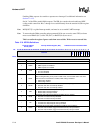
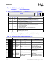
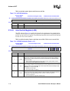
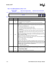
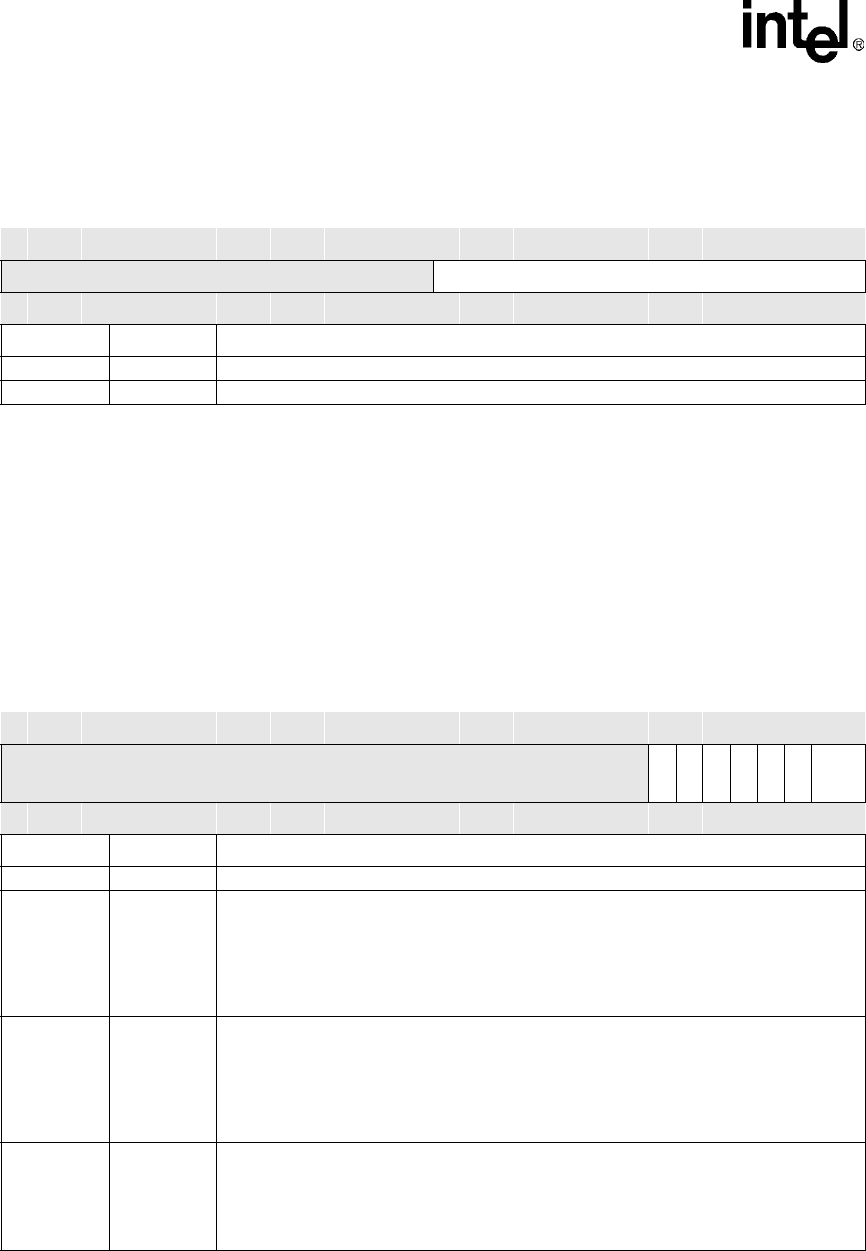
Table 17-13. ACR
Bit Definitions
Physical Address
0x4160_002C
Autobaud Count Register (ACR) PXA255 Processor Hardware UART
Bit
31 30 29 28 27 26 25 24 23 22 21 20 19 18 17 16 15 14 13 12 11 10 9 8 7 6 5 4 3 2 1 0
reserved Count Value
Reset
? ? ? ? ? ? ? ? ? ? ? ? ? ? ? ? 0 0 0 0 0 0 0 0 0 0 0 0 0 0 0 0
Bits Name Description
31:16 — reserved
15:0 ACR Number of 14.7456 MHz clock cycles within a start bit pulse.
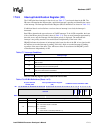
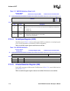
Table 17-14. LCR Bit Definitions (Sheet 1 of 2)
Physical Address
0x4160_000C
Line Control Register (LCR) PXA255 Processor Hardware UART
Bit
31 30 29 28 27 26 25 24 23 22 21 20 19 18 17 16 15 14 13 12 11 10 9 8 7 6 5 4 3 2 1 0
reserved
DLAB
SB
STKYP
EPS
PEN
STB
WLS
Reset ? ? ? ? ? ? ? ? ? ? ? ? ? ? ? ? ? ? ? ? ? ? ? ? 0 0 0 0 0 0 0 0
Bits Name Description
31:8 — reserved
7DLAB
DIVISOR LATCH ACCESS BIT
Must be set to access the divisor latches of the baud rate generator during a READ or
WRITE operation. Must be cleared to access the receiver buffer, the Transmit Holding
register, or the IER.
0 = Access Transmit Holding register (THR), Receive Buffer register (RBR) and IER.
1 = Access Divisor Latch registers (DLL and DLH)
6SB
SET BREAK
Causes a break condition to be transmitted to the receiving UART. Acts only on the TXD pin
and has no effect on the transmitter logic. In FIFO mode, wait until the transmitter is idle,
LSR[TEMT]=1, to set and clear SB.
0 = No effect on TXD output
1 = Forces TXD output to 0 (space)
5STKYP
STICKY PARITY
Forces the bit value at the parity bit location to be the opposite of the EPS bit, rather than
the parity value. This stops parity generation. If PEN = 0, STKYP is ignored.
0 = No effect on parity bit
1 = Forces parity bit to be opposite of EPS bit value