6-56 Intel® PXA255 Processor Developer’s Manual
Memory Controller
6.7.6 FLASH Memory Interface
The processor provides an SRAM-like interface for access of Flash memory. The RDF fields in the
MSCx registers are the latency for each read access to non-burst Flash, or the first read access to
burst Flash. The RDF fields also control the nWE low time during a write cycle to Flash. The RDN
field controls subsequent read access times to burst Flash and the nWE low time during a write
cycle to non-burst Flash. RRR is the time from nCS deassertion after a read to the start of a read
from a different memory, or after a write to another memory access.
Reads from Flash memory have the following requirements:
• Because Flash defaults to Read-Array mode, burst reads are permitted out of Flash, which
allows instruction caching and DMA reads from Flash.
• Software partitions commands and data and writes the commands to Flash before the read. The
Memory controller does not insert any commands before Flash reads.
Writes to Flash memory have the following requirements:
• Flash memory space must be uncacheable and unbuffered.
• Burst writes to Flash are not supported. Writes to Flash must be exactly the width of the
populated Flash devices on the data bus and must be a burst length of one write, for example
no byte writes to a 32-bit bus. The allowable writes are: 2 bytes written to a 16-bit bus, and 4-
bytes written to a 32-bit bus.
• For asynchronous writes to Flash, the command and data must be given in separate write
instructions to the Memory controller, the first carries the command, the next carries the data.
• The Memory controller does not insert any commands before Flash writes. Software must
write the commands and data in the correct order.
• No Flash writes can be bursts. DMA must never write to Flash.
For writes to Flash, if all byte enables are turned off (masking out the data, DQM = 1111), the write
enable is suppressed (nWE = 1) for the write beat, which can result in a period when nCS is
asserted, but neither nOE nor nWE is asserted. This happens when there is a 1-beat write to Flash,
but all byte enables are turned off.
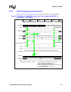
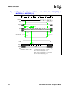
6.7.6.1 FLASH Memory Timing Diagrams and Parameters
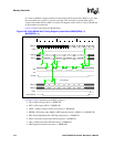
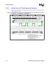
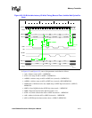
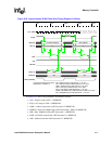
Non-burst Flash reads have the same timing as non-burst ROMs reads. Figure 6-23 shows the
timing for writes to non-burst asynchronous Flash.


