Intel® PXA255 Processor Developer’s Manual 7-9
LCD Controller
7.3.5.1 Passive Display Timing
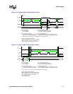
In passive display mode (LCCR0[PAS] = 0), L_PCLK toggles only when data is being written to
the panel. When an entire line of pixels has been sent to the display, L_LCLK is asserted. When an
entire frame of pixels has been sent to the display, L_FCLK is asserted.
If an output FIFO underrun occurs (i.e., the LCD controller runs out of data), L_PCLK stalls until
valid data is available. This results in a slower pixel clock, but data sent to the display is always
valid.
To prevent a D.C. charge from building within a passive display, its power and ground supplies
must be switched periodically. Many modern panels do this automatically. If not, the LCD
controller can toggle the AC bias pin (L_BIAS) to signal the display to switch the polarity. The
frequency of the L_BIAS toggle is controlled by programming the number of line clock transitions
between each toggle (LCCR3[ACB]).
7.3.5.2 Active Display Timing
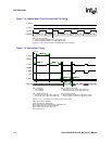
In active display mode (LCCR0[PAS] = 1), L_PCLK toggles continuously as long as the LCD
controller is enabled. The other pins function as follows:
L_BIAS — output enable. When asserted, the LCD latches L_DD data using L_PCLK.
L_LCLK — horizontal synchronization signal (HSYNC)
L_FCLK — vertical synchronization signal (VSYNC)
If an output FIFO underrun occurs, the data on the L_DD pins is repeated, L_BIAS stays asserted,
and L_PCLK keeps running. As valid data enters the output FIFO, it is sent to the display.
Additional pixel clocks are inserted at the end of the line to drain the remaining valid pixels from
the output FIFO before HSYNC is asserted. This mechanism allows an underrun to corrupt only a
single line rather than an entire frame.
7.3.5.3 Pixel Data Pins (L_DDx)
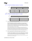
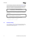
Pixel data is removed from the bottom of the output FIFO and driven in parallel onto the LCD data
lines on the edge of the pixel clock selected by Pixel Clock Polarity (LCCR3[PCP]). For a 4-bit
wide bus, data goes out on the LCD data lines L_DD[3:0]. For an 8-bit wide bus, data goes out on
L_DD[7:0]. For a 16-bit bus, data goes out on L_DD[15:0]. In monochrome dual-panel mode, the
pixels for the upper half of the screen go out on L_DD[3:0] and those for the lower half on
L_DD[7:4]. In color dual-panel mode, the upper panel pixels go out on L_DD[7:0] and the lower
panel pixels on L_DD[15:8].
The LCD data pins are driven at their last value during the inactive
portion of the LCD frame.
7.3.6 DMA
Values for palette RAM entries and encoded pixel data are stored in off-chip memory and are
transferred to the LCD controller’s input FIFO buffers, on a demand basis, using the LCD
controller’s dedicated DMA controller (DMAC). The LCD’s descriptor-based DMAC contains two
channels that transfer data from external memory to the input FIFOs. One channel is used for
single-panel displays and two are used for dual-panel displays.
The LCD controller issues a service request to the DMAC after it has been initialized and enabled.
The DMAC automatically performs eight word transfers, filling four entries of the input FIFO.
Values are fetched from the bottom of the FIFO, one entry at a time, and each 64-bit value is


