


6-44 Intel® PXA255 Processor Developer’s Manual
Memory Controller
The RT fields in the MSCx registers specify the type of memory:
• Non-burst ROM or Flash
• SRAM
• Variable Latency I/O
• Burst-of-four ROM or Flash
• Burst-of-eight ROM or Flash
The RBW fields specify the bus width for the memory space selected by nCS[5:0]. For a 16-bit bus
width transactions occur on MD[15:0]. The BOOT_SEL pins and/or SXCNFG register must be
used to configure nCS[3:0] for SMROM or some other type of Synchronous Static Memory.
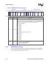
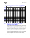
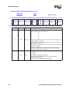
6.7.2 Asynchronous Static Memory Control Registers (MSCx)
The MSCx, shown in Table 6-21, are read/write registers and contain control bits for configuring
Static Memory (or Variable Latency I/O) that correspond to chip-select pairs nCS(1:0), nCS(3:2),
and nCS(5:4), respectively. Timing fields are specified as numbers of memory clock cycles. Each
of the three registers contain two identical CNFG fields One for each chip select in the pair.
When programming a different memory type in an MSC register, ensure that the new value has
been accepted and programmed before issuing a command to that memory. To do this, the MSC
register must be read after it is written and before an access to the memory is attempted. This is
especially important when changing from ROM/Flash to an unconstrained writable memory type
(such as SRAM).
If any of the nCS[3:0] banks is configured for Synchronous Static Memory via SXCNFG[SXENx],
the corresponding half-words of MSC0 and/or MSC1 are ignored, except MSCx:RBWx, the data
width. Another exception is non-SDRAM timing Synchronous Flash, which writes asynchronously
and requires these programmed values.
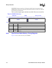
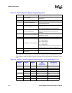
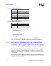
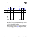
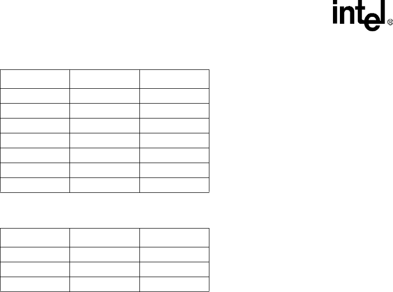
Table 6-19. 32-Bit Bus Write Access
Data Size MA[1:0] DQM[3:0]
8-bit 00 1110
8-bit 01 1101
8-bit 10 1011
8-bit 11 0111
16-bit 00 1100
16-bit 10 0011
32-bit 00 0000
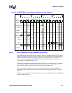
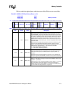
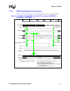
Table 6-20. 16-Bit Bus Write Access
Data Size MA[0] DQM[1:0]
8-bits 0 10
8-bits 1 01
16-bits 0 00