Intel® PXA255 Processor Developer’s Manual 6-7
Memory Controller
6.4 Memory Accesses
If a memory access is followed by an idle bus period, the control signals return to their inactive
state. The address and data signals remain at their previous values to avoid unnecessary bus
transitions and eliminate the need for multiple pull-up resistors.
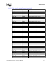
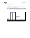
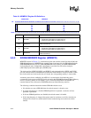
Table 6-1 lists all the transactions that the processor can generate. No burst can cross an aligned 32-
byte boundary. On a 16-bit data bus, each full word access becomes a two half-word burst, with
address bit 1 set to a 0. Each write access to Flash memory space must take place in one non-burst
operation, regardless of the bus size.
Table 6-1. Device Transactions
Bus Operation
Burst Size
(Words)
Start Address
Bits [4:2]
Description
Read single 1 Any Generated by core, DMA, or LCD request.
Read burst 4
0
4
Generated by DMA or LCD request.
Read burst 8 0 Generated by cache line fills.
Write single 1 Any
1..4 bytes are written as specified by the byte mask.
Generated by DMA request.
Write burst 2
0,1,2
4,5,6
All 4 bytes of each word are written. Generated by DMA
request.
Write burst 3
0,1
4,5
All 4 bytes of each word are written. Generated by DMA
request.
Write burst 4
0
4
All 4 bytes of each word are written. Generated by DMA
request.
Write burst 8 0 Cacheline copyback. All 32 bytes are written.


