Intel® PXA255 Processor Developer’s Manual 7-5
LCD Controller
If the LCD controller is being re-enabled, there has not been a reset since the last programming,
and the GPIO pins are still configured for LCD Controller functionality, only the registers
FDADRx and LCCR0 need to be reprogrammed. The LCD Controller Status Register (LCSR)
must also be written to clear any old status flags before re-enabling the LCD controller. See
Section 7.6.7 for details.
7.2.2 Disabling the Controller
The LCD controller can be disabled in two ways: regular and quick.
Regular disabling, the recommended method for stopping the LCD controller, is accomplished by
setting the disable bit, LCCR0[DIS]. The other bits in LCCR0 must not be changed — read the
register, set the DIS bit, and rewrite the register. This method causes the LCD controller to stop
cleanly at the end of the frame currently being fetched from memory. If the LCD DMAC is
fetching palette data when DIS is set, the palette RAM load is completed, and the next frame is
displayed before the LCD is disabled. The LCD Disable Done bit, LCSR[LDD], is set when the
LCD controller finishes displaying the last frame fetched, and the enable bit, LCCR0[ENB], is
cleared automatically by hardware.
Quick disabling is accomplished by clearing the enable bit, LCCR0[ENB]. The LCD controller
will finish any current DMA transfer, stop driving the panel, and shut down immediately, setting
the quick-disable bit, LCSR[QD]. This method is intended for situations such as a battery fault,
where system bus traffic has to be minimized immediately so the processor can have enough time
to store critical data to memory before the loss of power. The LCD controller must not be re-
enabled until the QD bit is set, indicating that the quick shutdown is complete.
Once disabled, the LCD Controller automatically disables its clocks to conserve power.
7.2.3 Resetting the Controller
At reset, the LCD Controller is disabled, and the output pins are configured as GPIO pins. All LCD
Controller Registers are reset to the conditions shown in the register descriptions.
7.3 Detailed Module Descriptions
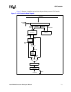
This section describes the functions of the modules in the LCD Controller:
7.3.1 Input FIFOs
Data fetched from external memory by the dedicated DMAC is placed in one of two input FIFO
buffers. Each input FIFO comprises 128 bytes, organized as 16 entries by 8 bytes. In single-panel
mode, one FIFO is used to queue both encoded pixel data and data for writing to the internal palette
RAM. In dual-panel mode, this FIFO queues data for the internal palette RAM and the upper half
of the LCD display, while the second FIFO buffer holds data for the lower half of the LCD display.
The FIFO signals a service request to the DMAC whenever four FIFO entries are empty. In turn,
the DMAC automatically fills the FIFO with a 32-byte burst. Pixel data from the frame buffer
remains packed within individual 8-byte entries when it is loaded into the FIFO. If the pixel size is


