Intel® PXA255 Processor Developer’s Manual 7-17
LCD Controller
7.6 Register Descriptions
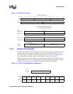
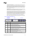
The LCD controller contains four control registers, ten DMA registers, one status register, and a
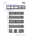
256-entry palette RAM. Table 7-16 lists their locations in physical memory. All of the LCD
registers must be accessed as 32-bit values. Reads and writes to undefined addresses in the LCD
register space yield unpredictable results and must not be attempted.
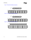
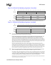
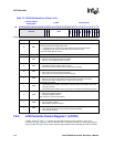
The control registers contain bit fields to do the following:
• Enable and disable the LCD controller.
• Define the height and width of the screen being controlled.
• Indicate single- or dual-panel display mode.
• Indicate color versus monochrome mode.
• Indicate passive versus active display.
• Set the polarity of the control pins.
• Set the pulse width of the line and frame clocks, pixel clock, and ac bias pin frequency.
• Set the AC bias pin toggles per interrupt.
• Set the number of wait states to insert before and after each line and after each frame.
• Enable various interrupt masks.
An additional control field exists to tune the DMAC’s performance based on the type of memory
system with which the processor is used. This field controls the placement of a minimum delay
between each LCD DMA request during palette loads to insure enough bus bandwidth is given to
other bus masters for accesses.
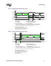
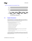
Figure 7-16. Active Mode Pixel Clock and Data Pin Timing
Pixel 0 Pixel 1 Pixel 2 Pixel 3 Pixel 4
PCP - Pixel Clock Polarity
0 - Pixels sampled from data pins on rising edge of clock.
1 - Pixels sampled from data pins on falling edge of clock
.
For PCP = 1 the L_PCLK waveform is inverted, but the timing is identical.
L_FCLK
(VSYNC)
L_LCLK
(HSYNC)
L_BIAS
(OE)
L_PCLK
LDD[15:0]
PCP = 0


