6-38 Intel® PXA255 Processor Developer’s Manual
Memory Controller
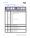
SXCNFG[RL] fields must match any CAS latencies and RAS latencies programmed in this
SXMRS register. Software must ensure that fields match the latencies. In some cases, duplicate
information must be programmed.
This is a read/write register. Ignore reads from reserved bits. Write zeros to reserved bits.
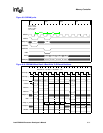
6.6.3 Synchronous Static Memory Timing Diagrams
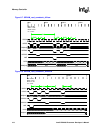
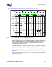
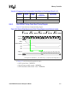
Figure 6-12 shows a three-beat read cycle for SMROM.
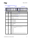
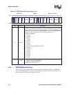
Table 6-16. SXMRS Bit Definitions
0x4800_0024 SXMRS Memory Controller
Bit
31 30 29 28 27 26 25 24 23 22 21 20 19 18 17 16 15 14 13 12 11 10 9 8 7 6 5 4 3 2 1 0
reserved
SXMRS2
reserved
SXMRS0
Reset
0 0 0 0 0 0 1 0 0 0 1 1 0 0 1 0 0 0 0 0 0 0 1 0 0 0 1 1 0 0 1 0
Bits Name Description
31 — reserved
30:16 SXMRS2
MRS value to be written to Synchronous Static memory requiring an MRS command for
Bank Pair 2
15 — reserved
14:0 SXMRS0
MRS value to be written to Synchronous Static Memory requiring an MRS command for
Bank Pair 0


