6-12 Intel® PXA255 Processor Developer’s Manual
Memory Controller
6.5.2 SDRAM Mode Register Set Configuration Register
(MDMRS)
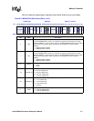
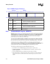
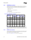
The MDMRS, shown in Table 6-3, issues an Mode Register Set (MRS) command to the SDRAM.
The value written in this register is placed directly on address lines MA[24:17] during the MRS
command. For MA[16:10], values which are fixed or derived from the MDCNFG register are
placed on the address bus. When setting the values to be written out on the address lines, base the
values on the addressing mode being used. Although writing to this register triggers an MRS
command, the corresponding chip-select values are asserted only if the memory banks are enabled
via the MDCNFG register. Therefore, to appropriately write a new MRS value to SDRAM, first
enable the memory via the MDCNFG register, and then write the MDMRS register. This register is
used solely for generating the MRS command.
All values in the MDCNFG register must be programmed correctly to ensure proper operation of
the device.
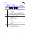
The MDMRS[MDBLx] bits configure the SDRAM to a burst length of four. This value is fixed and
cannot be changed. For transfer cycles that require more data than the set burst length of four, the
controller can preform as many bursts as necessary to transfer the required amount of data. For
example, during a cache line fill the controller can perform a four-beat burst followed immediately
by another four-beat burst. This approach requires the controller to generate the first address for the
second burst. During transfer cycles less than four beats, the controller ignores the data it does not
need. For instance, if the SDRAM is configured as non-cacheable, single beat reads are seen on the
bus as a four-beat read with only one beat that is used by the processor. This also applies to a
single-beat write.
This is a read/write register. Ignore reads from reserved bits. Write zeros to reserved bits.
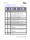
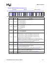
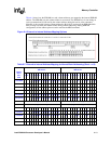
Table 6-3. MDMRS Bit Definitions (Sheet 1 of 2)
0x4800_0040 MDMRS Memory Controller
Bit
31 30 29 28 27 26 25 24 23 22 21 20 19 18 17 16 15 14 13 12 11 10 9 8 7 6 5 4 3 2 1 0
reserved
MDMRS2 MDCL2
MDADD2
MDBL2
reserved
MDMRS0 MDCL0
MDADD0
MDBL0
Reset
0 0 0 0 0 0 0 0 0 0 1 0 0 0 1 0 0 0 0 0 0 0 0 0 0 0 1 0 0 0 1 0
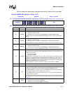
31 — reserved
30:23 MDMRS2 MRS value to be written to SDRAM for partition pair 2.
22:20 MDCL2
SDRAM partition pair 2 CAS Latency - derived from MDCNFG:DTC2. Writes are ignored.
Ready-only.
19 MDADD2
SDRAM partition pair 2 Burst Type. Fix to sequential addressing. Writes are ignored.
Always reads 0.
18:16 MDBL2
SDRAM partition pair 2 burst length. Fixed to a burst length of four. Writes are ignored.
Always reads 010.
15 — reserved
14:7 MDMRS0 MRS value to be written to SDRAM for Partition Pair 0.


