Intel® PXA26x Processor Family Developer’s Manual 4-3
System Integration Unit
4.1.2 GPIO Alternate Functions
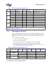
GPIO pins are capable of having as many as six alternate functions (shown Table 4-1) that can be
set to enable additional functionality within the processor. If a GPIO is used for an alternate
function, then it cannot be used as a GPIO at the same time. GPIO[0] is reserved because of its
special use during sleep mode and is not available for alternate functions. GPIO[15:0] are used for
sleep-mode wake up. The wake-up functionality is described in Section 3.4.9.5, “Exiting Sleep
Mode” on page 3-19. Table 4-1 shows each GPIO pin and its corresponding alternate functions.
For more information on alternate functions, refer to the source unit column in Table 4-1 for the
appropriate section of this document.
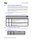
Table 4-1. GPIO Alternate Functions (Sheet 1 of 5)
Pin
Alternate
Function Name
Alternate Function
Assignment
AF{n}
encoding
Source Unit Signal Description and comments
GP1 GP_RST ALT_FN_1_IN 01
Clocks & Power
Manager Unit
Active low GP_reset
GP6 MMCCLK ALT_FN_1_OUT 01
Multimedia Card
(MMC) Controller
MMC Clock
GP7 48 MHz clock
†
ALT_FN_1_OUT 01
Clocks & Power
Manager Unit
48-MHz clock output
GP8 MMCCS0 ALT_FN_1_OUT 01
Multimedia Card
(MMC) Controller
MMC Chip Select 0
GP9
MMCCS1 ALT_FN_1_OUT 01 MMC Chip Select 1
USB_RCV ALT_FN_1_IN 01 Single Ended USB USB Device Controller RCV
GP10 RTCCLK ALT_FN_1_OUT 01
System Integation
Unit
real time clock (1 Hz)
GP11 3.6 MHz ALT_FN_1_OUT 01
Clocks & Power
Manager Unit
3.6-MHz oscillator out
GP12 32 KHz ALT_FN_1_OUT 01 32-KHz out
GP13 MBGNT ALT_FN_2_OUT 10
Memory Controller
memory controller grant
GP14 MBREQ ALT_FN_1_IN 01
memory controller alternate bus
master request
GP15 nCS_1 ALT_FN_2_OUT 10 Memory Controller Active low chip select 1
GP16 PWM0 ALT_FN_2_OUT 10 System Integration PWM0 output
GP17 PWM1 ALT_FN_2_OUT 10 PWM1 output
GP18 RDY ALT_FN_1_IN 01 Memory Controller Ext. Bus Ready
GP19 DREQ[1] ALT_FN_1_IN 01 Memory Controller External DMA Request
GP20 DREQ[0] ALT_FN_1_IN 01 External DMA Request
GP23 SCLK ALT_FN_2_OUT 10 SSP Serial Port SSP clock
GP24 SFRM ALT_FN_2_OUT 10 SSP Frame
GP25 TXD ALT_FN_2_OUT 10 SSP transmit
GP26 RXD ALT_FN_1_IN 01 SSP receive
GP27 EXTCLK ALT_FN_1_IN 01 SSP ext_clk


