15-26 Intel® PXA26x Processor Family Developer’s Manual
MultiMediaCard Controller
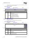
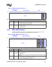
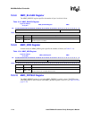
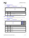
15.5.6 MMC_RESTO Register
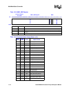
The MMC_RESTO register controls the number of MMC clocks that the controller must wait after
the command before it can turn on the time-out error if a response has not occurred (see
Table 15-11 on page 15-27). The default value of this register is 64.
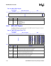
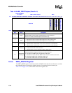
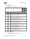
5BUSY
BUSY:
Specifies whether a busy signal is expected after the current command.
This bit is for no data command/response transactions only.
4
STREAM_BL
OCK
STREAM MODE:
0 – Data transfer of the current command sequence is not in stream mode
1 – Data transfer of the current command sequence is in stream mode
3 WRITE/READ
READ OR WRITE OPERATION:
0 – Specifies that the data transfer of the current command is a read operation
1 – Specifies that the data transfer of the current command is a write operation
2DATA_EN
DATA TRANSFER ENABLE:
0 – No data transfer with current command
1 – Specifies that the current command includes a data transfer
1:0
RESPONSE_
FORMAT[1:0]
RESPONSE FORMAT:
These bits specify the response format for the current command.
00 – No response in MMC mode. Not supported in SPI mode
01 – Format R1, R1b, R4, and R5 in MMC mode. Format R1 and R1b in SPI mode
10 – Format R2 in MMC mode. Format R2 in SPI mode
11 – Format R3 in MMC mode. Format R3 in SPI mode
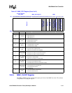
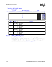
Table 15-10. MMC_CMDAT Register (Sheet 2 of 2)
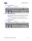
Physical Address
4110_0010
MMC_CMDAT Register MMC
Bit
31 30 29 28 27 26 25 24 23 22 21 20 19 18 17 16 15 14 13 12 11 10 9 8 7 6 5 4 3 2 1 0
Reserved
MMC_DMA_EN
INIT
BUSY
STREAM_BLOCK
WRITE/READ
DATA_EN
RESPONSE_FORMAT[1:0]
Reset 0 0 0 0 0 0 0 0 0 0 0 0 0 0 0 0 0 0 0 0 0 0 0 0 1 0 0 0 0 0 0 0
Bits Name Description


