7-34 Intel® PXA26x Processor Family Developer’s Manual
Liquid Crystal Display Controller
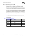
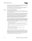
7.6.4.1 Double Pixel Clock (DPC)
DPC doubles the rate of the pixel clock on the L_PCLK pin. This allows direct connection to an
NTSC encoder (such as the Analog Devices 7171). All of the LCD controller settings are still
specified in terms of the original pixel clock and this mode affects only the L_PCLK output pin. If
DPC is set to 1, the pixel clock divisor (PCD) must be greater than or equal to 1.
7.6.4.2 Bits Per Pixel (BPP)
BPP specifies the size of encoded pixel values in memory. Pixel sizes of 1, 2, 4, and 8 bits require
the internal palette RAM be loaded before pixels can be displayed on the screen. See Section 7.6.5,
“LCD Controller DMA” for details on programming the DMAC to load the palette RAM. BPP is
programmed as:
0b000 = 1-bit pixels
0b001 = 2-bit pixels
0b010 = 4-bit pixels
0b011 = 8-bit pixels
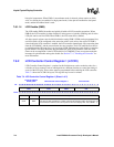
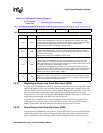
20 VSP
VERTICAL SYNC POLARITY (Section 7.6.4.6):
0 – L_FCLK pin is active high and inactive low.
1 – L_FCLK pin is active low and inactive high.
19:16 API
AC BIAS PIN TRANSITIONS PER INTERRUPT:
This value (0–15) specifies the number of AC bias pin transitions to count before setting the
line count status (ABC) bit, signalling an interrupt request. The counter is frozen when ABC
is set and is restarted when ABC is cleared by software. This function is disabled when
API=0x0.
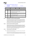
15:8 ACB
AC BIAS PIN FREQUENCY (Section 7.6.4.8):
In passive-display mode (LCCR0[PAS]=0), this value (0–255) specifies the number of line
clocks to count before toggling the AC bias pin. This pin is used to periodically invert the
polarity of the power supply to prevent D.C. charge buildup within the display. If the passive
display being controlled does not need to use L_BIAS, program ACB to its maximum value
(0xFF) to conserve power. ACB can be used in conjunction with API to count line clocks in
active mode (LCCR0[PAS]=1).
Number of line clocks/toggle of the L_BIAS pin = (ACB+1)
7:0 PCD
PIXEL CLOCK DIVISOR (Section 7.6.4.9):
This value (0–255) specifies the frequency of the pixel clock based on the LCD/memory
controller clock (LCLK) frequency. The pixel clock frequency can range from LCLK/2 to
LCLK/512.
Pixel clock frequency = LCLK/(2*(PCD+1)).
PCD must be programmed with a value of 1 or greater if double pixel clock mode is
enabled.
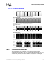
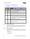
Table 7-6. LCD Controller Control Register 3 (Sheet 2 of 2)
Physical Address
0x4400_000C
LCD Controller Control Register 3 LCD Controller
Bit
31 30 29 28 27 26 25 24 23 22 21 20 19 18 17 16 15 14 13 12 11 10 9 8 7 6 5 4 3 2 1 0
reserved
DPC
BPP
OEP
PCP
HSP
VSP
API ACB PCD
Reset
X X X X 0 0 0 0 0 0 0 0 0 0 0 0 0 0 0 0 0 0 0 0 0 0 0 0 0 0 0 0
Bits Name Description


