Intel® PXA26x Processor Family Developer’s Manual 6-77
Memory Controller
being configured, the SDRAM banks must be disabled and MDREFR:APD must be
deasserted (auto-power-down disabled).
a. Write SXCNFG (with enable bits asserted).
b. Write to SXMRS to trigger an MRS command to all enabled banks of synchronous static
memory.
c. SXLCR must only be written when it is required by the SDRAM-like synchronous flash
device for command encoding.
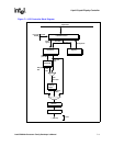
3. In systems that contain SDRAM, transition the SDRAM controller through this state
sequence:
a. self-refresh and clock-stop
b. self-refresh
c. power-down
d. PWRDNX
e. NOP
4. The SDRAM clock run and enable bits (MDREFR:K1RUN, K2RUN, and E1PIN), described
in Section 6.6.3. MDREFR:SLFRSH must not be asserted.
a. Write MDREFR:K1RUN, K2RUN (self-refresh and clock-stop -> self-refresh).
Configure MDREFR:K1DB2,K2DB2.
b. Write MDREFR:SLFRSH (self-refresh -> power-down).
c. Write MDREFR:E1PIN (power-down -> PWRDNX).
d. a write is not required for this state transition (PWRDNX -> NOP).
e. Configure, but do not enable, each SDRAM partition pair.
f. Write MDCNFG (with enable bits deasserted), MDCNFG:DE3:2,1:0 set to ‘0’.
5. For systems that contain SDRAM, wait a specified NOP power-up waiting period required by
the SDRAMs to ensure the SDRAMs receive a stable clock with a NOP condition
6. Ensure the Data Cache bit (DCACHE) is disabled. If this bit is enabled, the refreshes triggered
by the next step may not pass through to the Memory Controller properly.
7. On a hardware reset in systems that contain SDRAM, trigger the specified number (typically
eight) of refresh cycles by attempting non-burst read or write accesses to any disabled
SDRAM bank. Each such access causes a simultaneous CBR refresh cycles for all four banks,
which causes a pass through the CBR state and back to NOP. On the first pass, the PALL state
occurs before the CBR state.
8. Re-enable the DCACHE bit if it is disabled.
9. In systems that contain SDRAM, enable SDRAM partitions by setting
MDCNFG:DE3:2,DE1:0.
10. In systems that contain SDRAM, write the MDMRS register to trigger an MRS command to
all enabled banks of SDRAM. For each SDRAM partition pair that has one or both partitions
enabled, this forces a pass through the MRS state and back to NOP. The CAS latency must be
the only variable option and is derived from the value programmed in the
MDCNFG:MDTC0,2 fields. The burst type is programmed to sequential and the length is set
to four.


