Intel® PXA26x Processor Family Developer’s Manual 6-75
Memory Controller
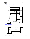
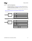
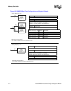
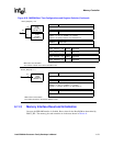
Figure 6-33. SMROM Boot Time Configurations and Register Defaults (Continued)
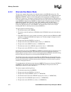
6.11.3 Memory Interface Reset and Initialization
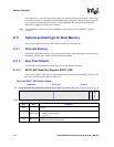
On reset, the SDRAM Interface is disabled. Reset values for the Boot ROM are determined by
BOOT_SEL. The memory pins and controller are in the state shown in Table 6-41.
BOOT_SEL[2:0] = 110
MSC0
SXCNFG
7FF0 7FF0
0004 4931
SXEN0 = 1h, SXCL0 = 4h (CL = 5),
SXRL0 = 1h (RL = 2), SXRA0 = 1h (13-bits),
SXCA0 = 2h (9-bits), SXTP0 = 0h, SXLATCH=1h
RBW0 = 0
MRS value must be 0061h.
BOOT_SEL[2:0] = 111
The number of banks in the device defaults to zero.
MDREFR 03CA 7FFF
E0PIN = 1, K0RUN = 1
SMROM
16-bit
(64 Mbit)
(nWORD = 0)
SMROM
16-bit
(64 Mbit)
(nWORD = 0)
16
16
32
MSC0
SXCNFG
7FF0 7FF8
0004 4531
SXEN0 = 1h, SXCL0 = 4h (CL = 5),
SXRL0 = 1h (RL = 2), SXRA0 = 1h (13-bits),
SXCA0 = 1h (8-bits), SXTP0 = 0h, SXLATCH=1h
RBW0 = 1
MRS value must be 0061h.
The number of banks in the device defaults to zero.
MDREFR 03CA 7FFF
E0PIN = 1, K0RUN = 1
SMROM
16-bit
(32 Mbit)
(nWORD = 0)
16
BOOT_SEL[2:0] = 100
BOOT_SEL[2:0] = 101
SXMRS
SXMRS
0232 0232
0232 0232
BOOT_SEL[2:0] = 110
BOOT_SEL[2:0] = 111
SXMRS
SXMRS
0232 0232
0232 0232


