Intel® PXA26x Processor Family Developer’s Manual 4-21
System Integration Unit
4.1.3.7 Example Procedure for Configuring the Alternate Function Registers
In this example, GP0 is used as a generic GPIO and GP(15:1) are configured as their alternate
functions. Refer to Table 4-1 for the list of alternate functions. No other GPIOs are configured.
After the de-assertion of any RESET, GPDR0(15:0) configures GPIO pins in this example to be
inputs. GAFR0_L(31:0) will be 0x0000_ 0000 to indicate normal GPIO function. For simplicity,
assume that GP(16:31) are inputs configured as normal GPIOs.
In this example,
• GPIO[0] is configured as a normal GPIO input
• GPIO[1] is an input configured to alternate function 1 (ALT_FN_1_IN)
• GPIO[5:2] are reserved and configured as normal GPIOs inputs
• GPIO[12:6] are outputs configured to alternate function 1 (ALT_FN_1_OUT)
• GPOI[13] is an output configured to alternate function 2 (ALT_FN_2_OUT)
• GPIO[14] is an input configured to alternate function 1 (ALT_FN_1_IN)
• GPIO[15] is an output configured to alternate function 2 (ALT_FN_2_OUT)
This programming sequence is required for programming the GPIO alternate functions out of reset:
1
. WRITE GPSR0 0x0000_8000 – this sets GPIO15 (active low chip select) when it is configured as an
outpu
t.
2. WRITE GPDR0 0x0000_BFC0
– GPIO[12:6], GPIO[13] and GPIO[15] as outputs. This drives
GPIO[15] high until the alternate function information is programmed. This is required for active
low outputs.
3. WRITE GAFR0_L 0x9955_5004
– this maps the alternate functions of GPIO[15:0]
For GPIOs that need to be configured as outputs, you must first program the GPSR and GPCR
signals so the pin direction is changed. Change pin direction by setting the bit in the GPDR
register
—a ‘0’ is driven for active high signals and ‘1’ for active low signals.
Note: For more information on alternate functions, refer to the Source Unit column in Table 4-1 for the
appropriate section of this document.
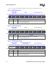
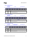
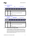
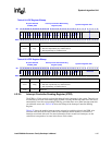
Table 4-24 through Table 4-29 show the bitmaps of the GPIO Alternate Function registers.
4.1.4 GPIO Register Locations
Table 4-30 shows the registers associated with the GPIO block and their physical addresses.
Table 4-30. GPIO Register Addresses (Sheet 1 of 2)
Address Name Description
0x40E0_0000 GPLR0 GPIO pin level register GPIO[31:0]
0x40E0_0004 GPLR1 GPIO pin level register GPIO[63:32]
0x40E0_0008 GPLR2 GPIO pin level register GPIO[89:64]
0x40E0_000C GPDR0 GPIO pin direction register GPIO[31:0]


