


6-72 Intel® PXA26x Processor Family Developer’s Manual
Memory Controller
is deasserted or, as part of the sleep entry routine, the alternate master can be disabled. If necessary,
the alternate master can hold the bus until its transaction is completed. After the memory controller
has completed all outstanding transactions, it places SDRAM into self-refresh and allows the
processor to complete the sleep entry sequence.
Note: The alternate bus master must de-assert MBREQ when nVDD_FAULT or nBATT_FAULT is
asserted.
6.11 Options and Settings for Boot Memory
This section explains the settings that control boot memory configurations.
6.11.1 Alternate Booting
The PXA261 and PXA262 allows only one boot configuration. This configuration is determined by
the BOOT_SEL[2:0] pins, which must be configured as 0b001.
6.11.2 Boot Time Defaults
The following sections provide information on boot time default parameters.
6.11.2.1 BOOT_DEF Read-Only Register (BOOT_DEF)
The read-only BOOT_DEF register contains the boot-up values for the three BOOT_SEL pins and
the single package-type bit. Refer to Table 6-40.
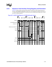
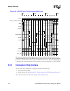
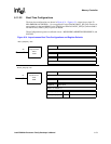
Table 6-40. BOOT_DEF Register Bitmap
0x4800 0044 BOOT_DEF Processor
Bit
31 30 29 28 27 26 25 24 23 22 21 20 19 18 17 16 15 14 13 12 11 10 9 8 7 6 5 4 3 2 1 0
Reserved
PKG_TYPE
BOOT_SEL
Reset 0 0 0 0 0 0 0 0 0 0 0 0 0 0 0 0 0 0 0 0 0 0 0 0 0 0 0 0 * * * *
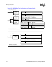
Bits Name Description
31:4 — Reserved
3 PKG_TYPE
PROCESSOR TYPE – This bit is READ ONLY.
1 – PXA26x processor family
0 – reserved
2:0 BOOT_SEL
PROCESSOR BOOT SELECT – Contains the three inputs pins BOOT_SEL[2:0] for the
processor. These bits are READ ONLY.