


Intel® PXA26x Processor Family Developer’s Manual 9-23
Inter-Integrated Circuit Bus Interface Unit
9.9.2 I
2
C Data Buffer Register- IDBR
The processor uses the I
2
C Data Buffer Register to transmit and receive data from the I
2
C bus. The
IDBR is accessed by the program I/O on one side and by the I
2
C shift register on the other. The
IDBR receives data coming into the I
2
C unit after a full byte is received and acknowledged. The
processor core writes data going out of the I
2
C unit to the IDBR and sends it to the serial bus.
When the I
2
C unit is in transmit mode (master or slave), the processor writes data to the IDBR over
the internal bus. The processor writes data to the IDBR when a master transaction is initiated or
when the IDBR Transmit Empty Interrupt is signalled. Data moves from the IDBR to the shift
register when the Transfer Byte bit is set. The IDBR Transmit Empty Interrupt is signalled (if
enabled) when a byte is transferred on the I
2
C bus and the acknowledge cycle is complete. If the
IDBR is not written by the processor and a STOP condition is not in place before the I
2
C bus is
ready to transfer the next byte packet, the I
2
C unit inserts wait states until the processor writes the
IDBR and sets the Transfer Byte bit.
When the I
2
C unit is in receive mode (master or slave), the processor reads IDBR data over the
internal bus. The processor reads data from the IDBR when the IDBR Receive Full Interrupt is
signalled. The data moves from the shift register to the IDBR when the ACK cycle is complete.
The I
2
C unit inserts wait states until the IDBR is read. Refer to Section 9.4.3, “Inter-Integrated
Circuit Acknowledge” for more information on the acknowledge pulse in receiver mode. After the
processor reads the IDBR, the ACK/NAK Control bit is written and the Transfer Byte bit is written,
allowing the next byte transfer to proceed to the I
2
C bus. The IDBR register is 0x00 after reset.
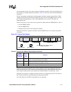
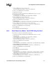
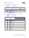
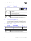
Table 9-9. I
2
C Bus Monitor Register - IBMR
Physical Address
4030_1680
I
2
C Bus Monitor Register I
2
C
Bit
31 30 29 28 27 26 25 24 23 22 21 20 19 18 17 16 15 14 13 12 11 10 9 8 7 6 5 4 3 2 1 0
Reserved
SCLS
SDAS
Reset 0 0 0 0 0 0 0 0 0 0 0 0 0 0 0 0 0 0 0 0 0 0 0 0 0 0 0 0 0 0 1 1
31:2 — Reserved
1SCLS
SCL STATUS:
This bit continuously reflects the value of the SCL pin.
0SDAS
SDA STATUS:
This bit continuously reflects the value of the SDA pin.
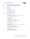
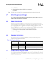
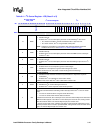
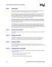
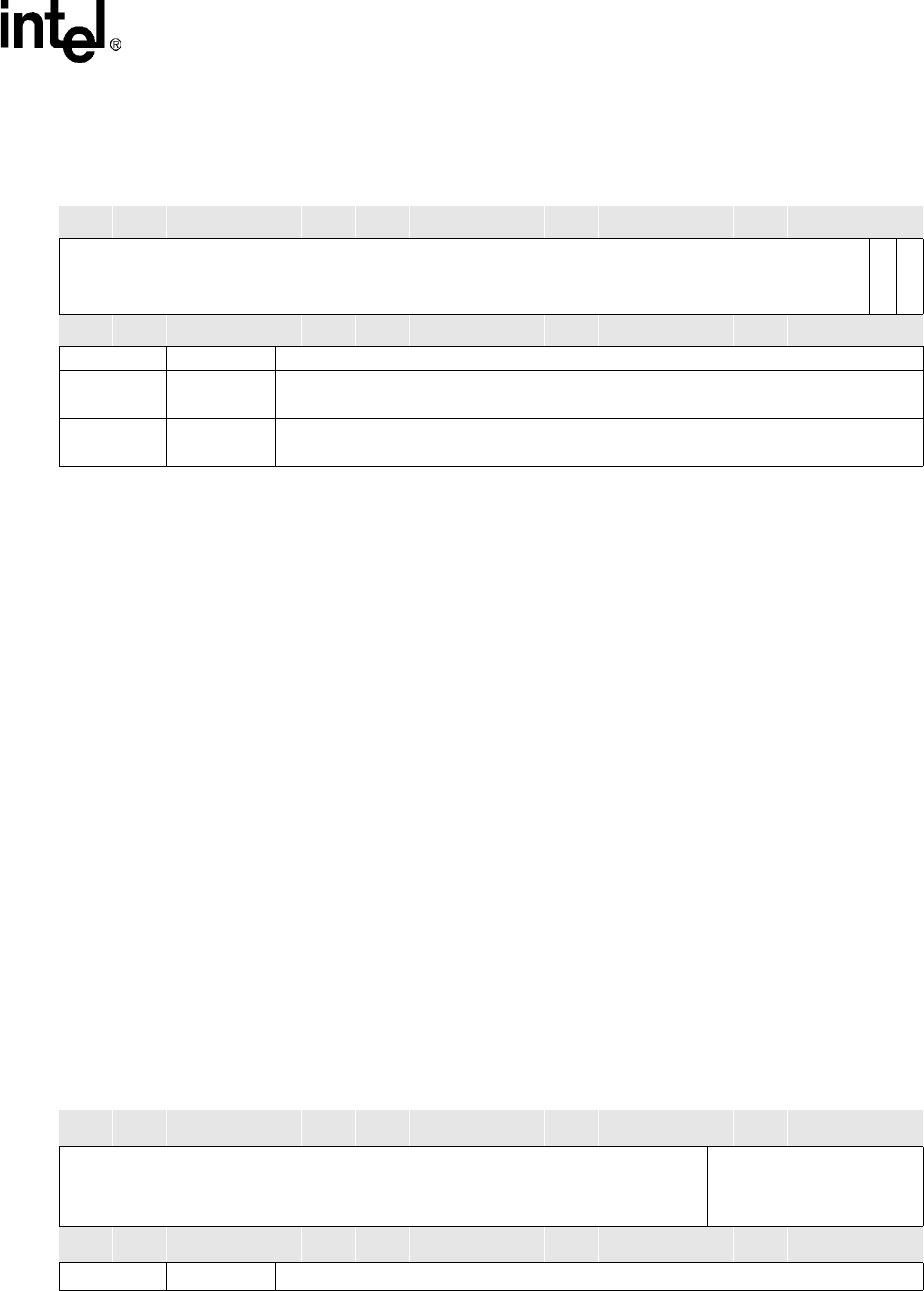
Table 9-10. I
2
C Data Buffer Register - IDBR (Sheet 1 of 2)
Physical Address
4030_1688
I
2
C Data Buffer Register I
2
C
Bit
31 30 29 28 27 26 25 24 23 22 21 20 19 18 17 16 15 14 13 12 11 10 9 8 7 6 5 4 3 2 1 0
Reserved
IDB
Reset 0 0 0 0 0 0 0 0 0 0 0 0 0 0 0 0 0 0 0 0 0 0 0 0 0 0 0 0 0 0 0 0
31:8 — Reserved