7-30 Intel® PXA26x Processor Family Developer’s Manual
Liquid Crystal Display Controller
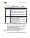
elapsed. When L_LCLK is asserted, the value in HSW is transferred to a 6-bit down counter, which
decrements at the programmed pixel clock frequency. When the counter reaches zero, L_LCLK is
negated. HSW can be programmed to generate a line clock pulse width ranging from 1 to 64 pixel
clock periods.
The pixel clock does not toggle during the line clock pulse in passive display mode but does toggle
in active display mode. The polarity (active and inactive state) of the line clock pin is programmed
using the horizontal sync polarity (HSP) bit in LCCR3.
HSW must be programmed with the desired number of pixel clocks minus one.
7.6.2.4 Pixels Per Line (PPL)
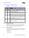
The pixels per line (PPL) bit-field specifies the number of pixels in each line or row on the screen
(minus one). PPL is a 10-bit value that represents between 1 and 1024 pixels per line. It is
recommended not to exceed 640 pixels. It counts the number of pixel clocks that must occur before
the line clock can be asserted. As discussed in Section 7.4.2, pixels per line must be multiples of:
32 pixels for 1-bit pixels, 16 pixels for 2-bit pixels, 8 pixels for 4-bit pixels, 4 pixels for 8-bit
pixels, and 2 pixels for 16-bit pixels. The two special conditions are: 8-bits per pixel monochrome
screens with double-pixel-data mode and 8 or 16 bits per pixel passive color screens require a
multiple of 8 pixels for each line.
If the display used is not naturally a multiple of the above, “dummy” pixels must be added to each
line to keep the frame buffer aligned in memory. For example, if the display being controlled is 250
pixels wide and the pixel-size is 8-bits, the nearest greater multiple of 8 is 256. Pixels per line must
be set to 255. 6 extra “dummy” pixel values must be added to the end of each line in the frame
buffer. The display being controlled must ignore the dummy pixel clocks at the end of each line.
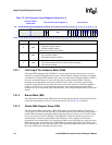
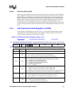
7.6.3 LCD Controller Control Register 2 (LCCR2)
LCD Controller Control Register 2 contains four bit fields that are used as values for a collection of
down counters, each of which performs a different function to control the timing of several of the
LCD’s pins. Table 7-5 shows the bit layout of LCCR2. This register is read/write.


