


Intel® PXA26x Processor Family Developer’s Manual 4-47
System Integration Unit
Note: Due to internal timing requirements, all changes to any of the PWM registers must be complete a
minimum of 4 core clock cycles before the start of end of a PWM clock cycle in order to guarantee
that the following PWM cycle implements the new values.
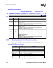
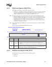
Table 4-52 shows the bitmap of the PWM Period Control registers.
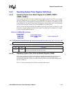
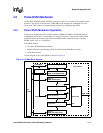
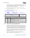
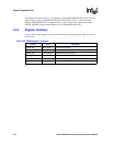
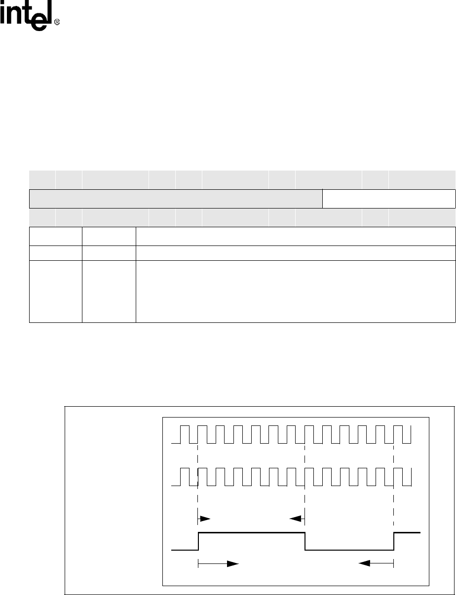
4.5.3 Pulse Width Modulator Output Wave Example
Figure 4-4 is an example of the output of a Pulse Width Modulator for reference.
PWM_PERVAL[PV] = 0xA
PWM_DUTY[FDCYCLE] = 0x0
PWM_DUTY[DCYCLE] = 0x6
PWM_CTRL[PRESCALE] = 0x0
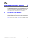
Table 4-52. PWM_PERVALn Bit Definitions
Physical Address
0x40B0_0008
0x40C0_0008
PWM Period Control Registers
(PWM_PERVAL0, PWM_PERVAL1)
System Integration Unit
Bit
31 30 29 28 27 26 25 24 23 22 21 20 19 18 17 16 15 14 13 12 11 10 9 8 7 6 5 4 3 2 1 0
Reserved PV
Reset
0 0 0 0 0 0 0 0 0 0 0 0 0 0 0 0 0 0 0 0 0 0 0 0 0 0 0 0 0 1 0 0
Bits Name Description
<31:10> — Reserved
<9:0> PV
PWMn PERIOD CONTROL:
The number of PSCLK_PWMn cycles that comprise one PWM_OUTn cycle
NOTE: If PV = 0x0, the PWMn clock (PWM_OUTn) is set high and does not toggle unless
FDCYCLE = 0x0 and DCYCLE = 0x0. In this case PWM_OUTn is set low and
does not toggle regardless of the value in PV.
Figure 4-4. Basic Pulse Width Waveform
PWM_OUTn
PSCLK_PWMn
PWM_DUTYn = 6
PWM_PERVALn = 10 (+1)
3.6864 MHz