12-24 Intel® PXA26x Processor Family Developer’s Manual
Universal Serial Bus Device Controller
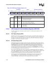
12.6.2 UDC Endpoint 0 Control/Status Register (UDCCS0)
The UDC endpoint zero control/status register contains 7 bits that operate endpoint zero, the
control endpoint.
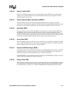
12.6.2.1 OUT Packet Ready (OPR)
The OUT packet ready bit is set by the UDC when it receives a valid OUT packet to endpoint zero.
When this bit is set, the USIR0[IR0] bit is set in the UDC status/interrupt register if endpoint zero
interrupts are enabled. This bit is cleared by writing a one. The UDC is not allowed to enter the
data phase of a transaction until this bit is cleared.
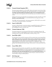
12.6.2.2 IN Packet Ready (IPR)
The IN packet ready bit is set by the core if less than max_packet bytes (16) have been written to
the endpoint 0 FIFO to be transmitted. The core must not set this bit if max_packet bytes are to be
transmitted. The UDC clears this bit when the packet has been successfully transmitted, the
UDCCS0[FTF] bit has been set, or a control OUT is received. When this bit is cleared due to a
successful IN transmission or the reception of a control OUT, the USIR0[IR0] bit in the UDC
interrupt register is set if the endpoint 0 interrupt is enabled via UICR0[IM0]. The core is not able
to clear UDCCS0[IPR] and always reads back a zero
When software enables the status stage for vendor/class commands and control data commands
such as GET_DESCRIPTOR, GET_CONFIGURATION, GET_INTERFACE, GET_STATUS, and
SET_DECSCRIPTOR, software must also set IPR. The data in the transmit FIFO must be
transmitted and the interrupt must be processed before the IPR is set for the status stage.
The status stage for all other USB Standard Commands that do not have a data stage, such as
SET_ADDRESS, SET_CONFIGURATION, SET_INTERFACE, SET_FEATURE, and
CLEAR_FEATURE, is handled by the UDC and the software must not set IPR.
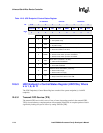
2RSM
DEVICE RESUME (read/write 1 to set):
0 – Maintain UDC suspend state
1 – Force UDC out of suspend
1UDA
UDC ACTIVE (read-only):
0 – UDC currently receiving a USB reset.
1 – UDC currently not receiving a USB reset.
0UDE
UDC ENABLE.(read/write):
0 – UDC disable.
1 – UDC enabled.
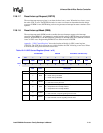
Table 12-12. UDC Control Register (Sheet 2 of 2)
0h 4060 0000 UDCCR Read/Write and Read-Only
Bit
31:8 7 6 5 4 3 2 1 0
Reserved REM RSTIR SRM SUSIR RESIR RSM UDA UDE
Rese
t
X 1 0 1 0 0 0 0 0
Bits Name Description


